December 2019
Connection/Development Board #1
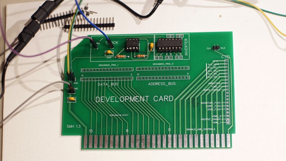
The first connection board has been partially assembled and was ready for the first round of tests to make sure my timer circuit works. For this first board, I setup a 10Hz astable 555 timer, with the the output going to a test pin. The output also goes to a 74LS04 hex inverter to give me a second, inverted, clock signal.
I tested by hooking channel 1 (yellow trace) of the oscilloscope to the 555 output, and channel 2 (purple) to the inverted 555 output.
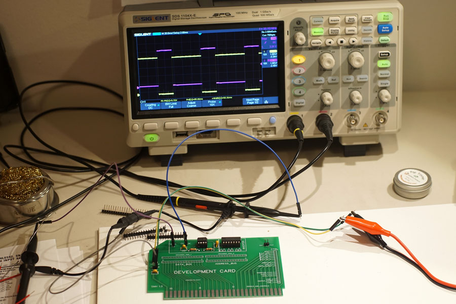
I adjusted the two channels to make it easy to see the two square waves, and it looks pretty good. The only possible concern is what appears to be a fair bit of noise when the signals are low. The long, unshielded test leads are probably responsible, but I plan on further testing.
All that remains is to solder on the 16-pin headers and this first connection/development board will be complete.
Connection/Development Board
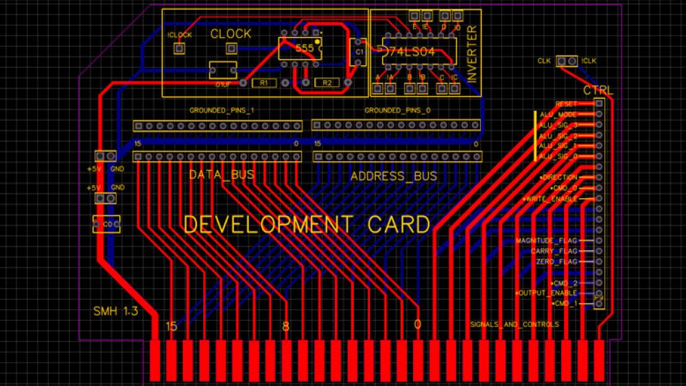
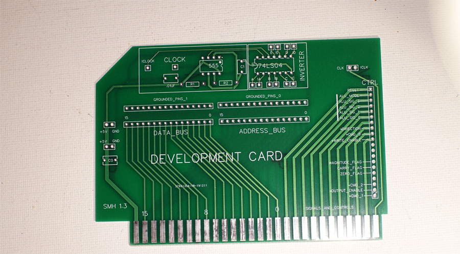
One of the issues when moving from breadboard to PCB is coming up with an interface between the two. To that end, I came up with a simple connection/development board that breaks all of the backplane lanes out to headers. To make development and testing easier, I added a 555 circuit, a hex inverter, and an extra set of grounded headers. The purpose of the grounded headers is to allow one of these boards to act as terminating resistors, pulling the buses low as a default. The 555 timer circuit allows us to have development clocks that can optionally be tied to the clock lanes of the backplane (again, via pin headers).
The main purpose of the connector board is to make it easy to connect to breadboards, so all of the headers are clearly labeled. Where labels are missing, the lane has not yet been assigned.
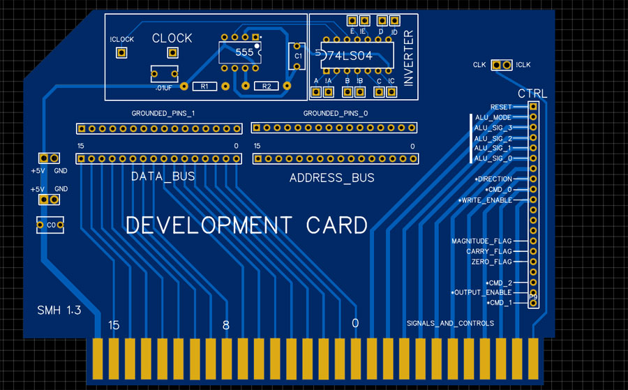
The most interesting part of this card is the labeled control header, as it sets a lot of things in stone. The rightmost connector lane is a common clock signal (on both sides of the card), but the next pads are not shared lanes, they are linked to the selector headers on the backplane. The rest of the signals and controls are lanes, including the ALU signals and the various flags. When I designed the board I was planning a minimum of three flags and was not sure what the third was going to be (A = B, A > B, A < B, Negative, etc), so I labeled it as the "Magnitude Flag", but it turns out that combining it with the carry flag can give us all three. There is room for more shared flags and controls.
Downloads
Connection Card 1.2 Gerber File
16-bit Hex Display Board
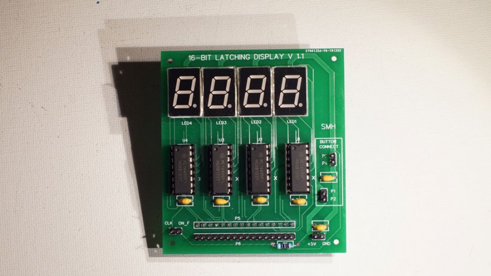
I have wanted a decent display system since I started this hobby in 2015, and finally had the opportunity to create something. The front-panel that I have planned will display binary output for the (control, signal, data, and address) buses, but will have four-digit hex displays for registers. The reason for this is it is much easier to quickly see values when they are displayed in hexadecimal, but binary is obviously better for showing which bits are set.
This display board was designed in EasyEDA, directly as a PCB... so no schematic. I probably should have created a schematic first, but I am a prototyper at heart and it feels better to me to lay out PCBs the way I lay out breadboards. I never draw circuits before breadboarding, so I am trying to do the same with these PCBs.
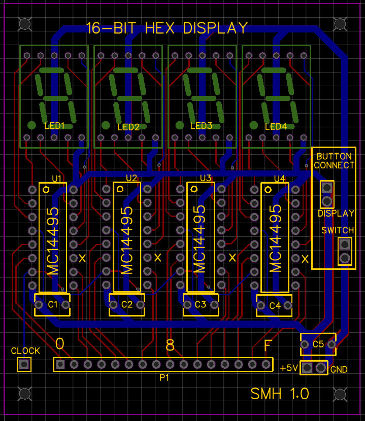
This is not the final version, but it is close and I wanted to compare it to the final version I had made. Because I do not do schematics, I end up laying out the PCB several times as I refine the components and positioning. This board is relatively simple, as it just needs four MC14995s to drive four 7-segment common cathode displays. I added a 16-pin header to connect the board, a clock pin, and power. Because I plan to use these with a front panel, there are pins to connect to controls... but for stand-alone use the switch pins can be shorted or jumpered. The decoupling capacitors are optional.
So, what was wrong with this design? Several things. First, I had planned to mount the displays on the reverse side, but I became confused during the layout and did not lay the traces 100% correctly. A second issue was the 16-pin header... really, I needed two so that the display could act as a pass-through.
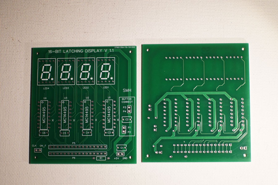
The final version is very similar to the 1.0 version, with the most notable exceptions being the displays and an extra 16-pin header. Front-panel related pin headers have been adjusted as well. The R1 resistor on the bottom of the board is a pull-up for the "on flag" pin.
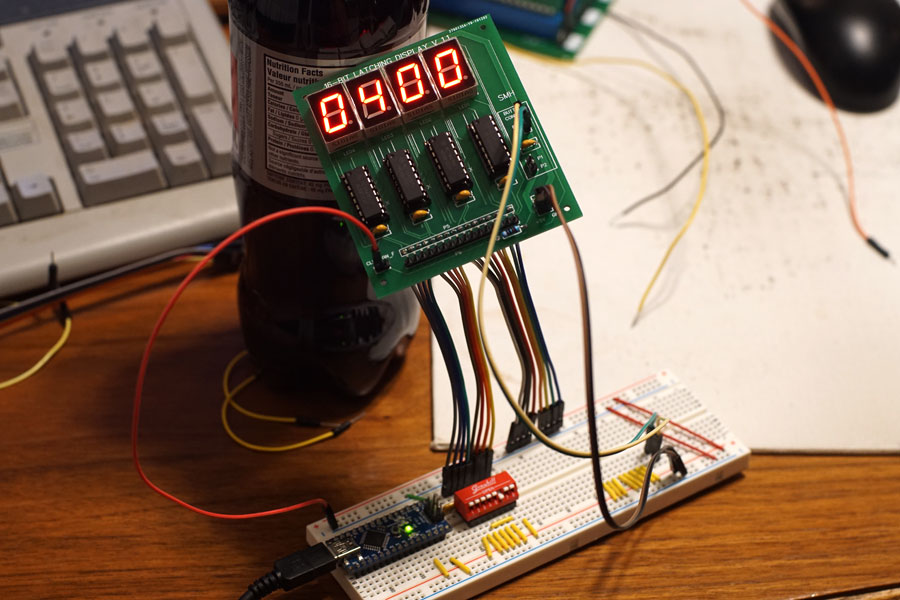
Fully populated, the hex display board was tested with a breadboard, 8-bits at a time (I only had one dip switch unit handy).
I have enough PCBs to build ten display boards, but I probably only need five or six, maybe a couple more for other projects.
Downloads
16-bit Register Board
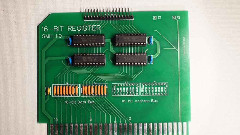
I had a lot of different plans for the 16-bit register, but all of them had two basic requirements:
- The PCB needs to work for both data-bus and address-bus registers.
- The PCB needs to have an "always on" header (for the front-panel or ALU)
I would prefer to design registers for specific uses, but when having PCBs manufactured it was more economical to try to combine designs as much as possible. Because of that, the PCB links the data and address-buses to the 74LS574 ICs, with breaks that I could jumper when populating the boards. To accomplish 3-state bus access but have the register value always available to a 16-pin header, I went with a second set of 74LS574s that store with the register ICs, but always outputs to the header. This adds about $2 to the cost of populating a register board, so in instances where the header might never be used, those extra ICs can be left out.
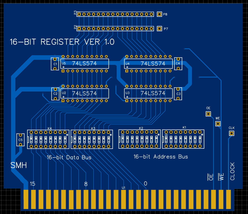
This design was created by hand as a PCB, without a schematic. I explain my reasoning in the Hex Display post, but basically I design PCBs the same way that I lay out breadboards... I grab the datasheets and start connecting pins. This is inefficient, and requires multiple iterations before I am happy with a design, but it feels better to me. In this case, this was not the final design but it makes an interesting contrast to what was produced. If you compare them, the main difference is how the signal test pins are located. The "clock" was dropped from this board, as the actual clock signal will be gated to this card and transmitted on the write enable line.
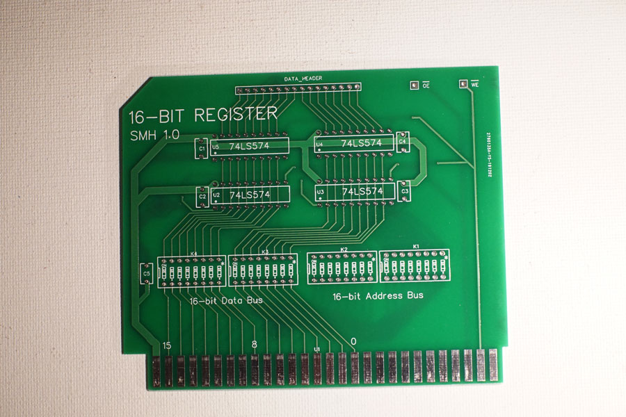
I also dropped the second 16-pin header on the top, as the display board was updated to act as a pass-through when necessary.
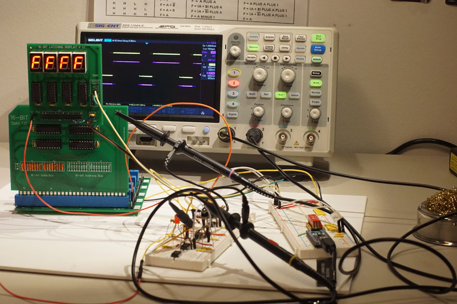
Fully populated, the register board was tested with my first display board. The oscilloscope probes are connected to the output of the 555 timer (on the foreground breadboard) and the clock test pin on the display board... I wanted to see how if the clock waveform deforms or picks up any noise. Unfortunately, when I took this photo I had the oscilloscope in "roll mode" so the waveform looks a bit dirty.
I have enough PCBs to build ten register boards, but I will start with three... A-Register and B-Register for the ALU, and one general purpose register. I might also populate an address register or two once I start programming branching and jumps.
Downloads
Backplane Connector Pinout (Schematic)
One of the nice things about designing PCBs to replace breadboards is we are forced to make decisions. Once a PCB is manufactured, it is not easy to make changes, where a breadboard is almost by definition always changing. This means that I am forced to finalize designs, so that all of the PCBs will work correctly.
In the case of the backplane, and the modified JAMMA connectors, there is some flexibility. I do not need to assign a purpose to every lane, but the shared lanes that are assigned must be respected by every card or device attached to the backplane. This has resulted in a series of pinout schematics, with the most recent displayed below.
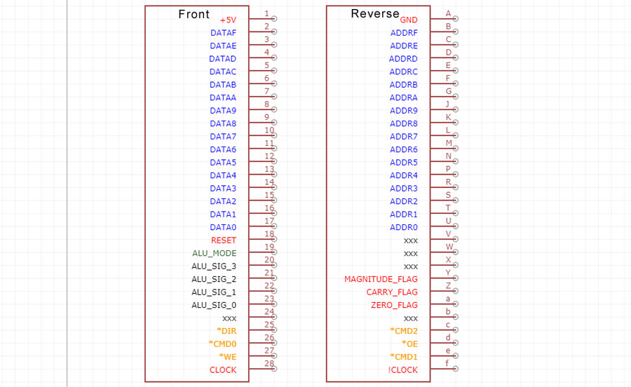
The front of the connector, and any PCBs inserted into the connector, is dominated by +5V, the 16-bit data bus, and the ALU signal lanes. The reverse is side has Ground, the 16-but address bus, and the flags. Each side also has three isolated breakout pins that are not shared between connectors. Note that the OE and WE pins are on opposite sites... this was caused by a layout error on the register card that was most easily fixed by reassigning the location of OE... even if it seems a little random when viewing the pinout. Whoops.
The "Reset" line is planned to be both user triggered (when the computer is turned on, or when a reset button is pressed) as well as software triggered. The purpose of reset would be to clear registers and set counters back to zero, so that a program can start "fresh". The software triggered reset is planned for future use... perhaps after a program is transferred from storage to ram, we clear the registers and start the program counter at the start of the program. In the case of "Reset", I plan to have a special purpose register that is not cleared... so that a program can react differently based on the contents of that register.
The ALU signals will be discussed at length elsewhere, but basically we have a mode flag that switches the 74LS181 ALU ICs between logical and mathematical functions, plus four command signals that select one of sixteen functions.
The six breakout pins, in orange, are unique to each card and can be assigned to anything, but the Write Enable and Output Enable are common for most devices so those are labelled. The DIR pin, and the three CMD pins are effectively unassigned at this time.
