StephenHermer.com
Writing, Iguanas, and Electronics

05 - Input/Output

Front Panel Instruction Indicators - Cardboard Prototype

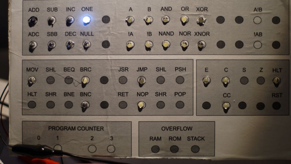
It is pretty rough, but this cardboard prototype of the "Instruction Indicators" panel will be pretty useful when I am working on control logic. I am working on the computer instructions / operations, and this will greatly speed development and allow easy confirmation that the control signals are correct.

Making a prototype was also helpful to identify some issues with the current design, including how impossibly bright the LEDs are. The illuminated LED in the above photo has two layers of opaque plastic covering it. I will be experimenting with dips and coating in the coming weeks, but the best option may be to power the LEDS from a separate 3-volt system to improve the lifespan of the LEDs.

Comments
Login to post comments.

Instructions and Indicator LEDS

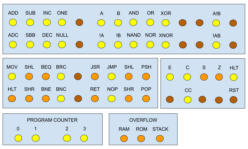
I will go over the actual operations and flags in detail, in future posts. For now, I just want to talk briefly about the blocks as currently envisioned. Before I do, there are three colours of LEDs in the graphic, as follows:

Yellow   - Planned to be implemented in the first phase.
Orange - Planned to be implemented in the second phase.
Brown   - Set aside for future use.

ALU Block
The ALU takes a 5-bit control word and does not require any additional control or decoding logic, so it is trivial to implement ALU functionality. This block is basically broken into three sections:

Left      - Arithmetic...          A plus B
Centre - Logic                    A XOR B
Right   - Complex Logic     A AND NOT B

Command Block
This block contains indicators for non-ALU operations, and includes things like register copy, jumps, branches, and stack related functions

Flags Block
This block, to the right of the Command Block, displays the flag indicators. The carry flag can be cleared, and thus there is a separate indicator for that. Indicators for system halt and reset round this block out.

Program Counter Block
This block contains the four dedicated counters assigned for RAM and ROM addressing, in two pairs. Normally only one counter will be active at a time.

Overflow Block
This block contains three indicators that will be illuminated when RAM addressing overflows, when ROM addressing overflows, and when the Stack Pointer overflows. Note that an overflow error will be thrown for an "under flow" as well; any time an address counter rolls over or resets an error will be thrown.

Comments
Login to post comments.

Card Pans - Block Diagrams

This is the "planned" architectural design for my card-based computer. The Control logic will not be a card slotted into the backplane, but pretty much everything else will be. I need to learn more about the various sound chips to lay out a sound card, but I imagine it will be complicated. I have dropped the Address Bus from the design as too limiting, but have not reallocated those 16-lanes yet... perhaps an I/O bus?I am not including any real details about flags or control here, to keep things simple... this is basically just an overview with block diagrams laid out to kind of look like the cards.
 
 
Register.jpg
 
The general purpose register card is already designed and manufactured, with three of them assembled and working. These are very basic devices, and might end up being entirely replaced by counters or shift-registers for efficiency purposes (if any register can be incremented or shifted, we save having to copy values from the general purpose register to the special register, perform the operation, and copy back). The general purpose register will also act as an interface for I/O operations... buffering front-panel input and holding "output" values for 7-segment displays.
 
I expect there to be at least four general purpose registers.
 
 
Counter.jpg
 
The counter card can read and write the data bus via transceivers, as the ICs used are not 3-state. This allows the ALU to write directly to the counter, after a jump or branch calculation. The counter always outputs to a pair of headers and supports increment, decrement, and reset signals. I think this design needs to generate an out-of-bounds signal, when the counter rolls from 0000 to FFFF or from FFFF to 0000.

I expect there will be several counters, optimally two for RAM, two for ROM, and one for the Stack. If we include a separate "Return Address Stack", that will require a counter to drive the address as well.
 
Feb19_Counter_Plus.jpg
 
I am prototyping an alternate counter card that includes a dedicated adder and  "offset-register" to make relative jumps easy and efficient. This would require some extra controls to change the offset register, but could save a lot of clock cycles when compared to using the ALU to calculate relative jumps. This design would need e out-of-bounds signal generation based on overflow or underflow from the adder logic to detect when the address rolls over (the address being somewhat independent of the actual counter value).
 
I expect there will be several counters, optimally two for RAM, two for ROM, and one for the Stack. If we use two stacks, that would require a sixth counter for the second stack. Not all counters would need to support offsets, but in those cases the outputs from the 74LS193a can be jumpered directly to the address output headers.
 
 
Shift-Register.jpg
 
The shift register card is very similar to the counter card, with the exception being that bits are shifted left or right instead of values being incremented or decremented.
 
 I expect there to be only one shift register needed.
 
 
RAM.jpg
 
The RAM card can rad from or output to the data bus via transceivers. While the RAM is 3-state, it is CMOS based and the transceivers will provide needed buffering of the bus. Addressing has been moved from the backplane to a pair of headers, controlled by transceivers or "one of two 4-bit word selectors", allowing for efficient addressing changes.
 
I expect there to be at least one RAM card, but will need an additional one for the Stack, and possibly a third for a "Return Stack"... if the stack is divided for efficiency purposes. 
 
ROM.jpg
 
The ROM card is functionally identical to the RAM card, as the EEPROMs and SRAM ICs used have identical pinouts and control signal requirements. While technically writable, the plan is to have a firmware card that does not receive WE signals from the control logic. 
 
The current plan is to have two ROM cards, one as firmware (to contain useful functions that can be called from user programs in RAM), and one that can act as storage (with the WE signal enabled to store programs).
 
 
Feb19_ALU_fixed.jpg
 
The ALU can write to the data bus via a buffer register (the 74LS181 is not 3-state). It receives inputs via sets of headers for the "A" input and the "B" input. The design was to have "A" and "B" simply be registers, but I plan to experiment with making them selectable, so that one input could toggle between a register and a counter (like the PC), while the other could toggle between a pair of registers. This would allow for more efficient calculations and comparisons without needing to spend cycles moving values between registers).
 
There will be a single ALU in the computer, but it may be cost-effective to design the ALU in halves for PCB manufacture (minimum orders are five PCBs).
Comments
Login to post comments.

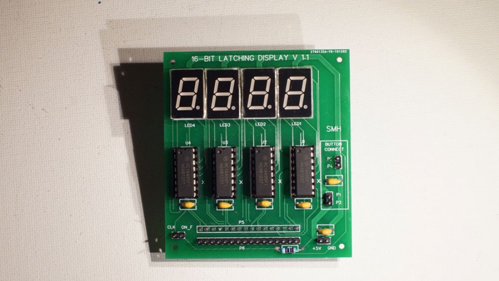
16-bit Hex Display Board

I have wanted a decent display system since I started this hobby in 2015, and finally had the opportunity to create something. The front-panel that I have planned will display binary output for the (control, signal, data, and address) buses, but will have four-digit hex displays for registers. The reason for this is it is much easier to quickly see values when they are displayed in hexadecimal, but binary is obviously better for showing which bits are set.

This display board was designed in EasyEDA, directly as a PCB... so no schematic. I probably should have created a schematic first, but I am a prototyper at heart and it feels better to me to lay out PCBs the way I lay out breadboards. I never draw circuits before breadboarding, so I am trying to do the same with these PCBs.

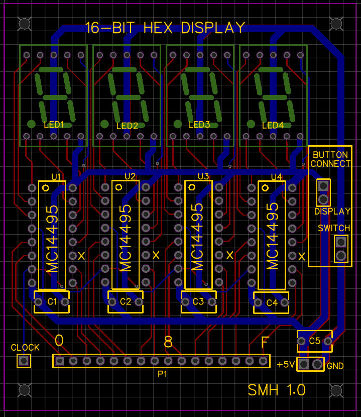
This is not the final version, but it is close and I wanted to compare it to the final version I had made. Because I do not do schematics, I end up laying out the PCB several times as I refine the components and positioning. This board is relatively simple, as it just needs four MC14995s to drive four 7-segment common cathode displays. I added a 16-pin header to connect the board, a clock pin, and power. Because I plan to use these with a front panel, there are pins to connect to controls... but for stand-alone use the switch pins can be shorted or jumpered. The decoupling capacitors are optional.

So, what was wrong with this design? Several things. First, I had planned to mount the displays on the reverse side, but I became confused during the layout and did not lay the traces 100% correctly. A second issue was the 16-pin header... really, I needed two so that the display could act as a pass-through.

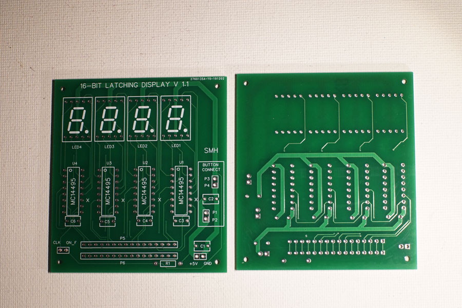
The final version is very similar to the 1.0 version, with the most notable exceptions being the displays and an extra 16-pin header. Front-panel related pin headers have been adjusted as well. The R1 resistor on the bottom of the board is a pull-up for the "on flag" pin.

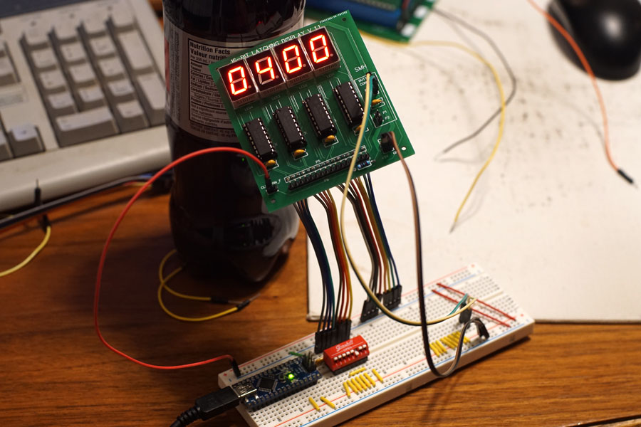
Fully populated, the hex display board was tested with a breadboard, 8-bits at a time (I only had one dip switch unit handy).

I have enough PCBs to build ten display boards, but I probably only need five or six, maybe a couple more for other projects.

Downloads

Hex Display 1.1 Gerber File

Comments
Login to post comments.