00 - Backplane
Bus Architecture - February 2020 Design
As I work through plans for the control logic and instructions, I realize that I need to simplify and streamline things. This does not mean lots of registers or segmented memory, or dropping a stack, but it does mean I am looking closely at how those things will work.
Six months ago, I was considering a two data bus, single address bus system with registers, pointers, memory, and even the ALU accessing at least two of the three buses. I like this because I could have an "A" and a "B" data bus that work as the inputs to the ALU. This simplified some things, and seemed like an elegant solution to the problems of moving data. Unfortunately, a three-bus system requires more control logic and a lot of transceivers, not to mention all of those extra traces that had to fit into two layers (I am not planning on moving to four-layer PCBs, lol).
Three months ago, I settled on a two bus system with address and data buses on the backplane. On paper this seemed the perfect solution, and seemed to be a common one in TTL based computers of the 70s and 80s. Again, there were difficulties with the two buses super-imposed on the backplane... complicated traces, extra transceivers, etc.
A more pressing concern with a common address bus is bus contention. I plan on having a bank of RAM, a bank of ROM, and later one of two Stacks. Each of these will need their own addressing, and if I want to be able to push a value onto a stack from RAM, it would be nice to have separate addressing so we can perform a single clock-cycle transfer (similar to copying values between registers).
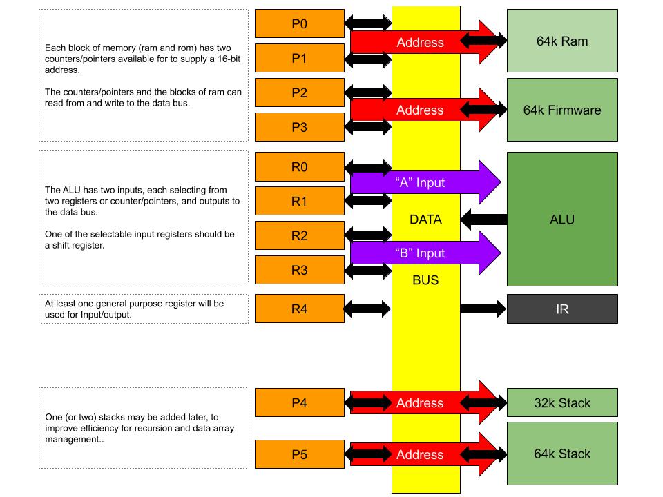
With the exceptions of the Instruction Register and Arithmetic Logic Unit, every device can read from and write to the data bus. With separate addressing for the memory based devices, we can copy values from any device (again, except the IR and ALU) in a single step. RAM to Register, Register to Pointer, Pointer to Stack, Stack to RAM, etc. The control logic is pretty simple, with each device having a write and load signal to control access to the data bus. In the case of RAM and ROM, I plan to have two pointers that can be selected from. Until a Stack is added, this will be the only efficient method to store a "return address" when performing a jump. Even after a Stack has been added, this will be more efficient when recursion is not evident.
The ALU has two inputs, labeled "A" and "B". In this design, these will have a choice of one of two inputs, much like the address lines for the memory cards. Multiple possible inputs mean we can save juggling data between registers, and if one of those registers is an address pointer, it means the ALU can calculate jumps and write them back to the address pointer very efficiently.
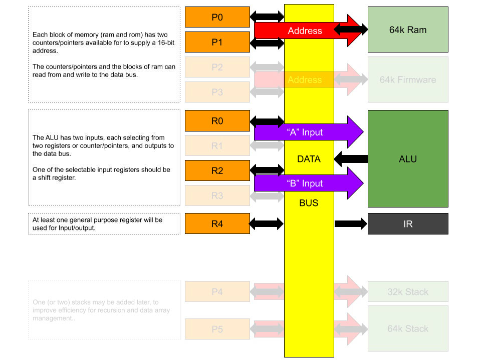
To start, we will only need one bank of memory with the pointers, the ALU with two input registers, one general purpose register (for output), and the Instruction Register. This will be enough to get started with.
New Modular Card Design
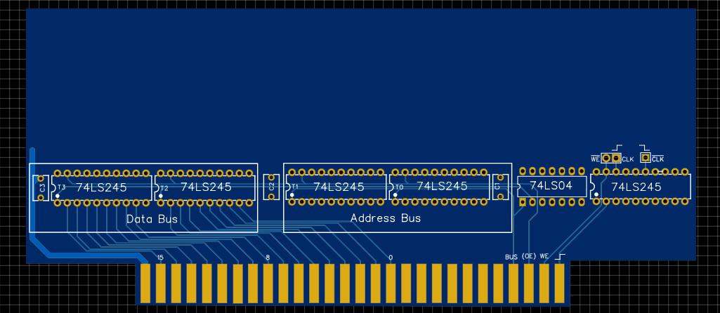
I have discovered some issues with the PCB designs I have had manufactured, and part of the issue is a lack of consistency. Take bus access, for example. The register card has placement for soldered wires or DIP switches to connect the register to the data or address bus. This is a bit limiting, but works and greatly reduces complexity. The memory card is even less complex, with the data pins linked to the data bus and the address pins linked to the address bus. When it comes to the counters, I want more flexibility to use them on either bus and as transfer registers between the buses. If the ALU can write to either bus, it can act as a partial transfer register... but it will need to be able to read from either bus for this to be useful.
Signals and Bus Termination
I remember learning about SCSI controllers, and hearing about termination. At the time I did not know what it meant, just that SCSI cables needed to be terminated for "some reason". The same is true for the computer I am building, the backplane (particularly the two two 16-lane buses) needs termination as well.
What is termination? Why do I need it?
In my case, termination really means pull-down and pull-up circuitry to eliminate glitches caused by floating voltages.
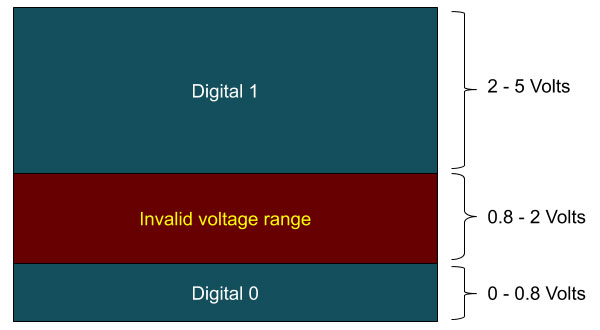 In theory, the computer is digital, passing values of "0" and "1" around... but in reality, it is an analog device where a certain voltage range indicates a "0" and another voltage range indicates a "1". Between these two ranges, there are voltages that are effectively invalid.
When voltages float between 0.8 and 2 volts, the computer will react unpredictably. Voltages are, at least in a computer like I am building, difficult to keep at exact levels.. transistors switching on and off, leaking voltages from ICs, even noise from outside the computer can add up to an "invalid" voltage reaching the low or high range and triggering an unwanted "0" or "1" response.
To prevent floating voltages from leading to problems, we will use pull-down and pull up resistors. A pull-down resistor is just a resistor between the floating pin or lane and ground. This effectively increase the voltage range that will be treated as a digital "0", by lowering the voltage by an amount. For example, if a -1 volt pull-down is implemented, a digital "0" will be seen for any voltage applied to that pin or late between 0 and 1.8 volts.
There is a lot of interesting math one can use to calculate the appropriate values for pull-down and pull-up resistors, but I am a prototyper so you will not see that math here. Instead, I try various resistor values until I find ones that work.
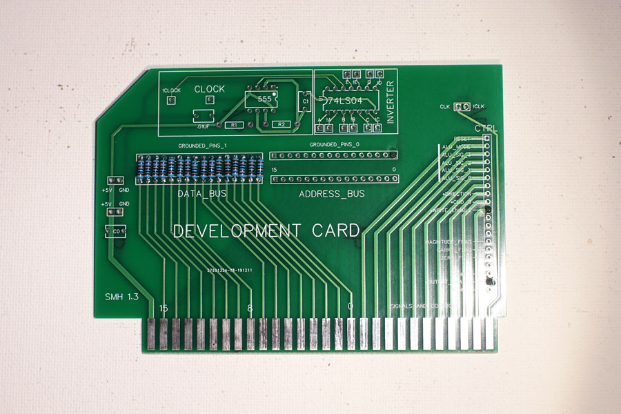
Using a connection/development board, I have added1k resistors between the 16-lanes of the backplane and ground. The purpose of this is to pull the bus low as a default, and 1k is a compromise for the first attempt.
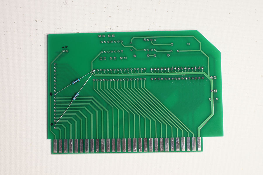
I also added 1k pull-down resistors to the Output Enable and Write Enable signals on this card, for testing purposes. These pins are not shared , so they will not act as pull-downs for any other card... but I have some tests in mind that they will be useful for.
The next step is to set the computer back up and test moving values between resistors again.
Connection/Development Board #1
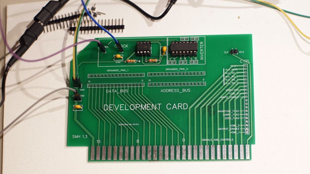
The first connection board has been partially assembled and was ready for the first round of tests to make sure my timer circuit works. For this first board, I setup a 10Hz astable 555 timer, with the the output going to a test pin. The output also goes to a 74LS04 hex inverter to give me a second, inverted, clock signal.
I tested by hooking channel 1 (yellow trace) of the oscilloscope to the 555 output, and channel 2 (purple) to the inverted 555 output.
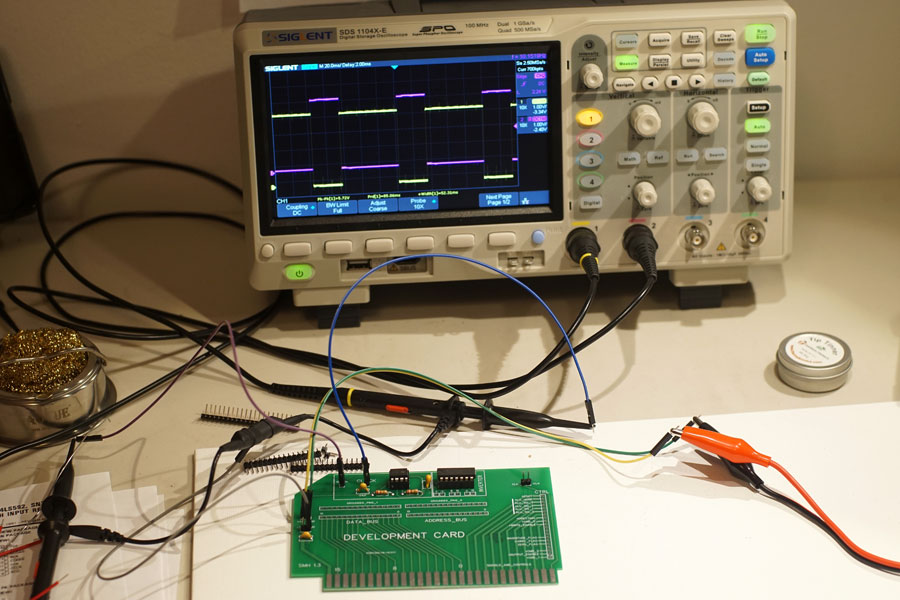
I adjusted the two channels to make it easy to see the two square waves, and it looks pretty good. The only possible concern is what appears to be a fair bit of noise when the signals are low. The long, unshielded test leads are probably responsible, but I plan on further testing.
All that remains is to solder on the 16-pin headers and this first connection/development board will be complete.
Connection/Development Board
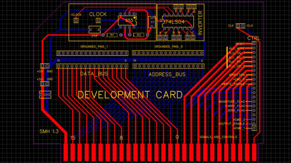
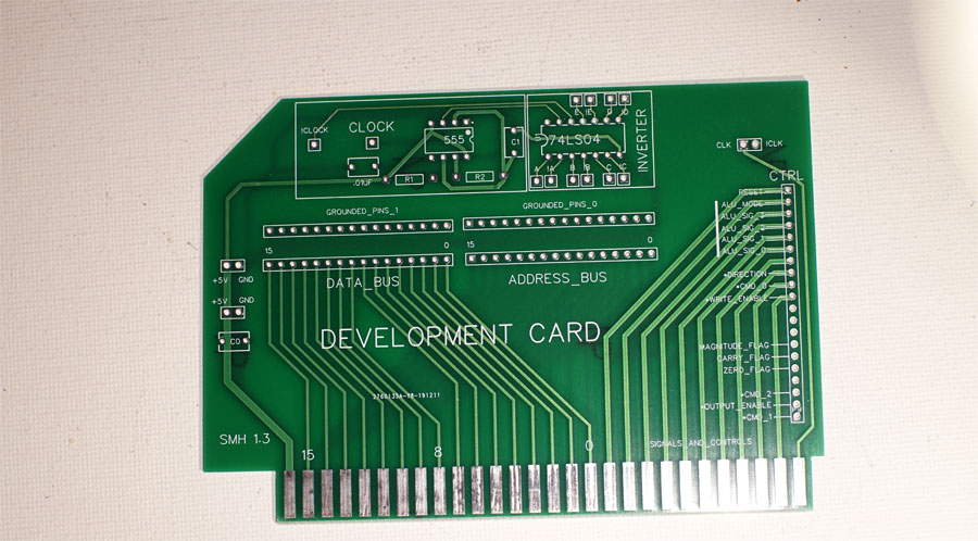
One of the issues when moving from breadboard to PCB is coming up with an interface between the two. To that end, I came up with a simple connection/development board that breaks all of the backplane lanes out to headers. To make development and testing easier, I added a 555 circuit, a hex inverter, and an extra set of grounded headers. The purpose of the grounded headers is to allow one of these boards to act as terminating resistors, pulling the buses low as a default. The 555 timer circuit allows us to have development clocks that can optionally be tied to the clock lanes of the backplane (again, via pin headers).
The main purpose of the connector board is to make it easy to connect to breadboards, so all of the headers are clearly labeled. Where labels are missing, the lane has not yet been assigned.
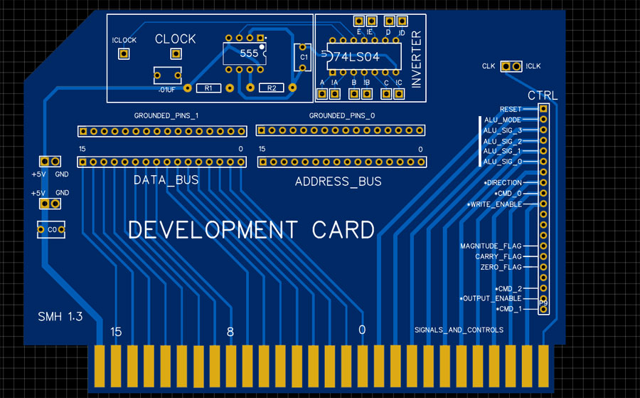
The most interesting part of this card is the labeled control header, as it sets a lot of things in stone. The rightmost connector lane is a common clock signal (on both sides of the card), but the next pads are not shared lanes, they are linked to the selector headers on the backplane. The rest of the signals and controls are lanes, including the ALU signals and the various flags. When I designed the board I was planning a minimum of three flags and was not sure what the third was going to be (A = B, A > B, A < B, Negative, etc), so I labeled it as the "Magnitude Flag", but it turns out that combining it with the carry flag can give us all three. There is room for more shared flags and controls.
Downloads
Connection Card 1.2 Gerber File
Backplane Connector Pinout (Schematic)
One of the nice things about designing PCBs to replace breadboards is we are forced to make decisions. Once a PCB is manufactured, it is not easy to make changes, where a breadboard is almost by definition always changing. This means that I am forced to finalize designs, so that all of the PCBs will work correctly.
In the case of the backplane, and the modified JAMMA connectors, there is some flexibility. I do not need to assign a purpose to every lane, but the shared lanes that are assigned must be respected by every card or device attached to the backplane. This has resulted in a series of pinout schematics, with the most recent displayed below.
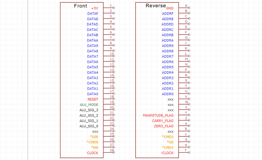
The front of the connector, and any PCBs inserted into the connector, is dominated by +5V, the 16-bit data bus, and the ALU signal lanes. The reverse is side has Ground, the 16-but address bus, and the flags. Each side also has three isolated breakout pins that are not shared between connectors. Note that the OE and WE pins are on opposite sites... this was caused by a layout error on the register card that was most easily fixed by reassigning the location of OE... even if it seems a little random when viewing the pinout. Whoops.
The "Reset" line is planned to be both user triggered (when the computer is turned on, or when a reset button is pressed) as well as software triggered. The purpose of reset would be to clear registers and set counters back to zero, so that a program can start "fresh". The software triggered reset is planned for future use... perhaps after a program is transferred from storage to ram, we clear the registers and start the program counter at the start of the program. In the case of "Reset", I plan to have a special purpose register that is not cleared... so that a program can react differently based on the contents of that register.
The ALU signals will be discussed at length elsewhere, but basically we have a mode flag that switches the 74LS181 ALU ICs between logical and mathematical functions, plus four command signals that select one of sixteen functions.
The six breakout pins, in orange, are unique to each card and can be assigned to anything, but the Write Enable and Output Enable are common for most devices so those are labelled. The DIR pin, and the three CMD pins are effectively unassigned at this time.
Backplane PCB
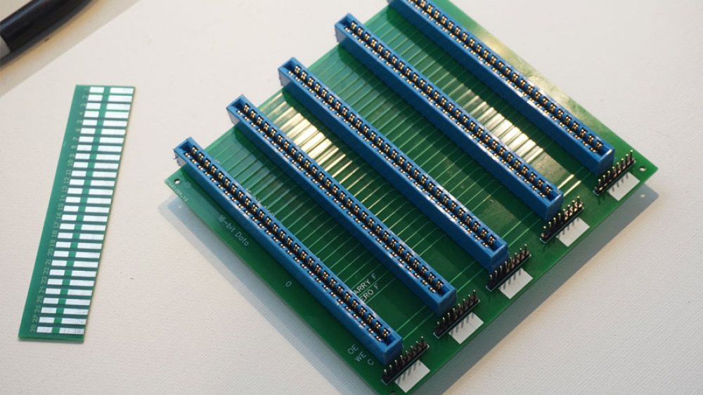
I ordered five backplane PCBs, and received them on November 27th. They turned out really well, except I did not leave space for the screw mounts on the ends of each JAMMA edge connector. The solution involved cutting the screw months off with a hacksaw, but the end result was the first two backplanes soldered and 100% tested.
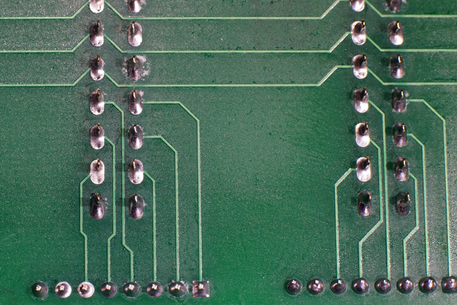
My soldering skills are pretty low, but the results turned out okay. The zoomed in shot shows the 6-lane breakout point for two of the connectors.
Downloads
Backplane Design
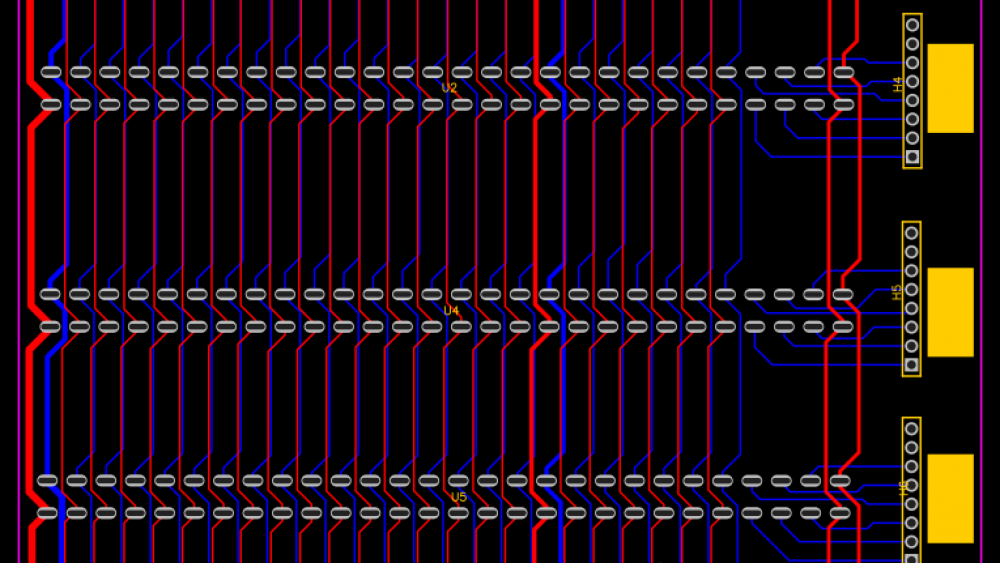
My first PCB design is the backplane, as it is relatively simple and will be needed by every subsequent PCB. It took a couple months of research, but I settled on JAMMA style edge connectors giving me a total of fifty-six lanes between the cards. I decided to break six lanes out to separate "card select" headers, so only fifty lanes are tied in parallel across the edge connectors.
To keep costs down, each board contains only five JAMMA connectors, plus pinheaders. I should have designed interconnects, to make linking boards easier, but the end result is a backplane allowing a maximum of twenty-five connected devices. I will need to order additional (or replacement) PCBs to expand beyond twenty-five connections, but I do not expect to need more than twelve or fifteen.
16-bit CPU - Backplane Concept
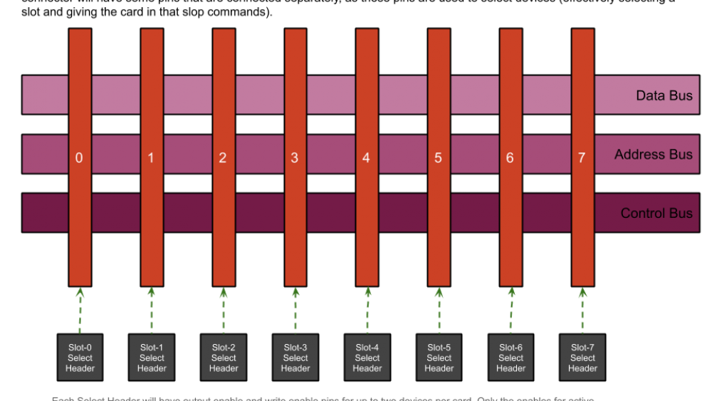
After a month of crazy plans and ideas, I settled on the idea of a backplane providing access to a 16-bit data bus, a 16-bit address bus, clocks, power, and control buses.
