01 - Register/Counter
Card Pans - Block Diagrams
I expect there will be several counters, optimally two for RAM, two for ROM, and one for the Stack. If we include a separate "Return Address Stack", that will require a counter to drive the address as well.
EEPROM Test
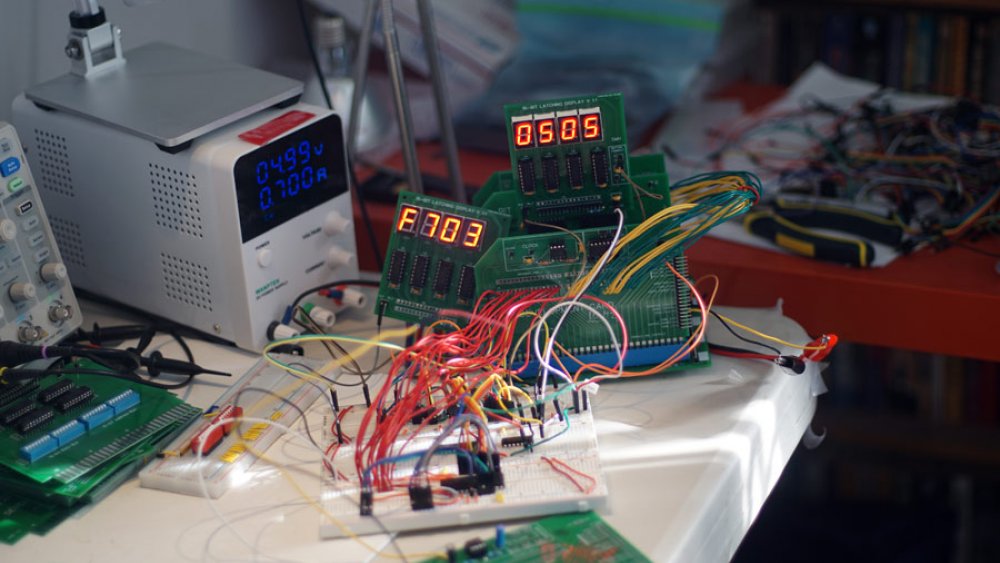
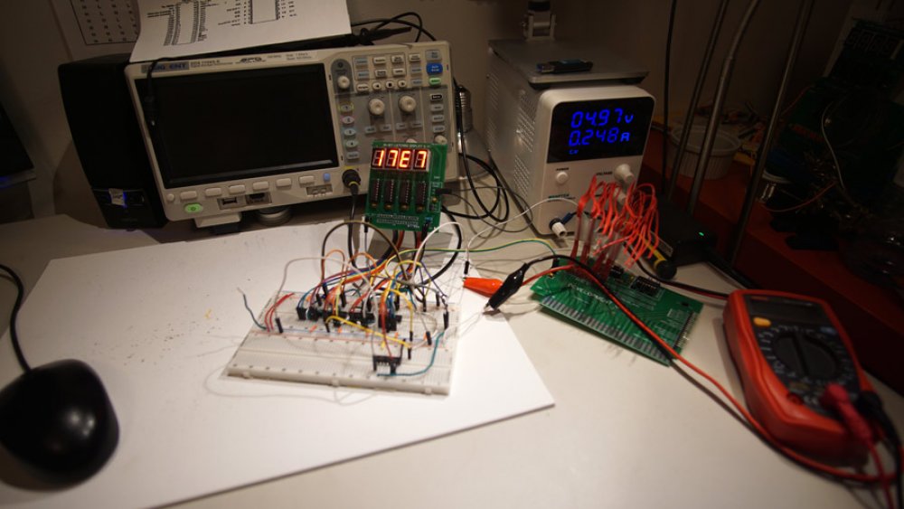
I know it looks like a mess, and it is, but this test of the 74LS193 counters driving an eeprom was a success. The counters and eeprom are located on the breadboards, the left display is showing the current address (the output of the 74LS193 counters), and the right display is showing the stored value in the "A" register. Because the "A" register is latching with the clock, it always contains the output of the eeprom (the eeprom writes to the data bus, and the "A" register is reading from it).
16-bit Counter PCB Design
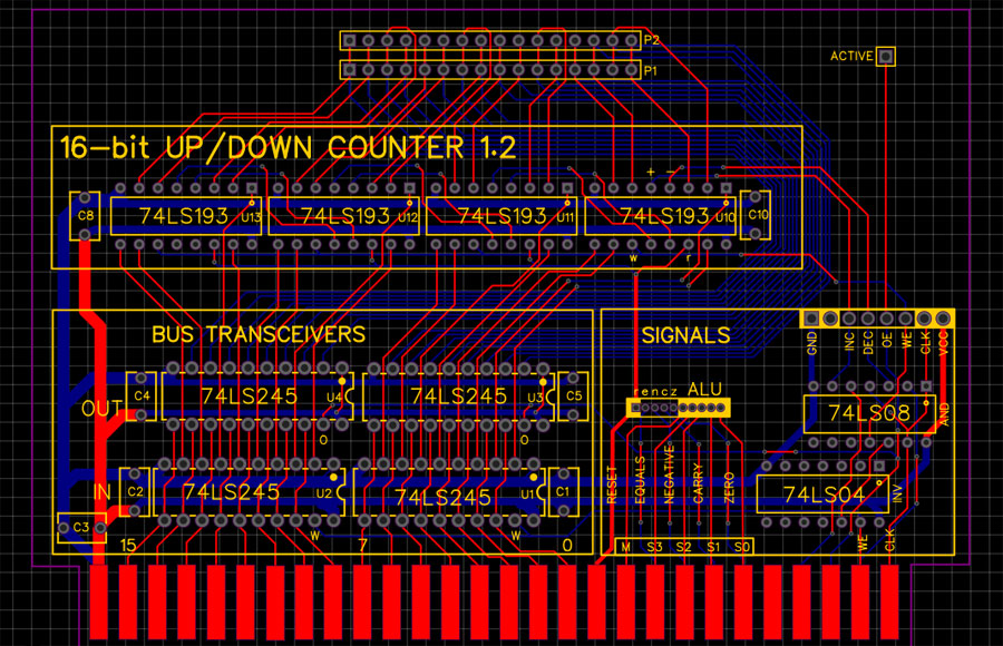
I have been struggling with planning the control logic of the computer, and a big part of that was handling the two buses. Some ICs, for example, the 74LS574 I use for registers, are 3-state. With a 3-state IC, the output can be disabled, and thus the inputs and outputs can be tied directly to a bus. In the case of the 74LS574 based registers, I want them to always output to a separate header, so I use transceivers to control access to the bus. With ICs that are not 3-state, we have no choice but to use transceivers, or they would always be outputting to the bus...even when we did not want them to. A second issue is that we need to separate the input from the output, otherwise these ICs output would interfere with the input values we want to store. Because of this, we need transceivers on both the input and output of our "card" to ensure that the card does not cause problems for other devices in the computer.
With a 16-bit data bus and a 16-bit address bus, I need four 74LS245 transceivers for 3-state devices, and six for the others. The cost of the extra transceiver ICs is not an issue (I have nearly sixty of them lol), but the PCB traces quickly get out of hand and the control logic to enable, disable, and set direction for all of them is complex.
The address bus has always been problematic in my design. I want to have multiple counters that can be enabled and disabled (for jumps, returns, etc), and I have multiple blocks of RAM and ROM that I want to be able to access. To that end, I have made the difficult decision to dispense with the address bus. This means that counter cards will need output headers (similar to the register cards), and new RAM or ROM cards will need to accept addressing from a similar header.
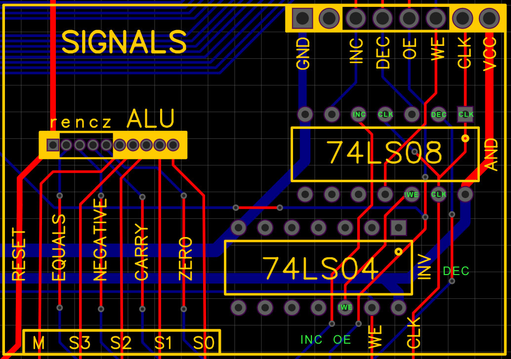
Without an address bus to worry about, we only need four transceivers, and because of that, we can stack them above the data bus and run all of the controls without any difficulty. The 74LS08 (quad AND gates) is used to gate the clock signals. If the WE signal is set, the CLK and !CLK signals are allowed through, otherwise no clock signals are available to the card. This has several benefits, including reducing the "fan out load" on the clock. All of the other signals and controls are passed through without buffering. The left controls (Flags and ALU lines) are only used on some cards, so buffering will only be added on appropriate cards. The right controls are not bused, so they do not need buffering. To keep things consistent, the "Write Enable" signal is active low (same as the Output Enable", but we need to invert it if we want to AND it with the clock. If the AND gate received a low "WE" signal, it would not pass the clock through, and thus no write would occur. We also need to and the Increment and Decrement signals with the clock, but those are already active high so we can bypass the hex inverter (74LS04). I have added some additional labels in green to make it easier to follow in the closeup shot.
16-bit Counter Prototype - Round Two
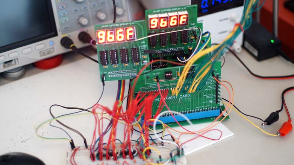
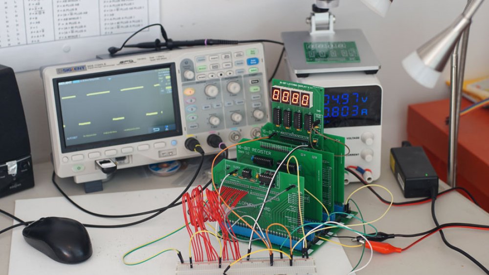
The 16-bit counters are successfully driving registers and displays attached to the backplane. I did some testing with the "autorouted" SRAM card, but I only had the data bus connected. For this test, I was running the 10Hz clock and all controls were via the appropriate connections (i.e. the backplane), except where the breadboard was involved.
The display on the left is connected directly to the outputs of the four 74LS193 counters on the breadboard. The counters get power and the clock (via the 74LS08 "gate") from the development card (at the front of the backplane). The red lines between the breadboard and the development card link to the backplane's data bus. The development card has the 555 timer circuit providing the clock to the backplane and the breadboard. The display on the right is attached to the monitor header of a 16-bit register card, and displays the output from the register. The ram card (not visible in the photo) was storing the data bus value at whatever random addresses the 16-unconnected wires was generating.
This test was to ensure the bus was working correctly, and that timing issues do not appear (at low frequencies, anyway). The next step will be to test writing to memory, then reading the values back. I do not have an input rig setup, so I will probably end up using an arduino for data reading and later checking.
16-bit Counter Prototype Testing
I made some modifications to the counter prototype, including gating the clock with a 74LS08 (quad AND gates), but it seems to have picked up some quirks. I was not able to adequately test at 10Hz... it was just fast enough to make it hard to catch errors with the naked eye, but just too slow for my oscilloscope. I ended up soldering up a second 555 based clock, this time running at a sedate 0.5Hz, giving me nearly two seconds to see each increment or decrement.
At the slower speed the issue became clear. The low 4-bits were displaying values out of order, and the issue turned out to be a couple of crossed jumper wires between the first counter IC and the first mc14995 display driver. Those crossed wires should have been an obvious place to start, but at 10Hz I could not tell the first digit was displaying values out of order, I was barely able to see that it seemed to skip values.
The interesting part to all of this is I learned of a limitation of oscilloscopes (or at least, the Siglent 1104X-E), namely they cannot "scope" frequencies below 10Hz. I honestly had no idea there was a lower limit.
BONUS CONTENT
I tested my first live-stream on Sunday, Feb 2nd, and while the stream is boring (and I do not recommend you watch much of it), the working counter is displayed for the first portion. The distortion and feedback was caused by a friend's video-chat.
I may do live-streams in the future, but they will be planned... I'll be prepared.
16-bit Counter Prototype
The original 8-bit computer design used the 74LS561 counter for the program counter. The 561 is definitely capable, but it is also a bit complex with synchronous and asynchronous operation in a 20-pin package. I tried using a few counters, but the ones I settled on are the 74LS193. This little 16-pin IC allows for loading, resetting to zeros, increment, and decrement. Most of the counter I tried are increment only, including the 561, so I ordered twently 193s and started prototyping when they arrived.
As you can see from the video (or the thumbnail, I won't judge), the 16-bit 193-based counter is working. I tested with load, clear, increment, and decrement successfully. This was with a 10Hz clock provided by the development board (middle, right, with all of the unconnected red wires), and I used one of the 4-digit hex displays for output.
The breadboard wiring looks complicated, but it worked almost perfectly from the start. A problem I did have was with the first 193 not counting. I eventually replaced it to the same effect and finally removed it. This necessitated adding a new forth IC to the left and moving the display wires, but the result was a successful prototype.
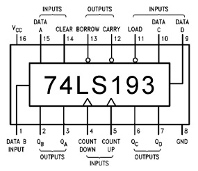
This IC is pretty simple, with a decent pin out. My preference would be for the data pins to be together and in order, but that is seldom the case with TTL components. The main things to look at with this IC are the count up/down pins, and the borrow/carry pins, as these are used to chain the ICs together to create a bigger counter... four of them, for a 16-bit version.
The increment and decrement signals are connected to the count up/down pins of the first (lowest 4-bits) counter IC. The carry from that counter is connected to the count up pin of the next IC, while the borrow is connected to the count down of the next IC. This is the same for the next two ICs, as they carry pin of one is connected to the count up of the next, and so on.
When incrementing, the counter will count to 15 before rolling back to a zero. When it does this, it sends a signal on the carry pin, which acts as the count up for the next IC. So, the first IC increments on every clock (10 times per second, in my prototype), but the second IC increments sixteen times slower.
Status and Control Register
There are various flags that need to be set for the computer to work correctly, such as a carry flag when an arithmetic operation results in a value larger than 16-bits.
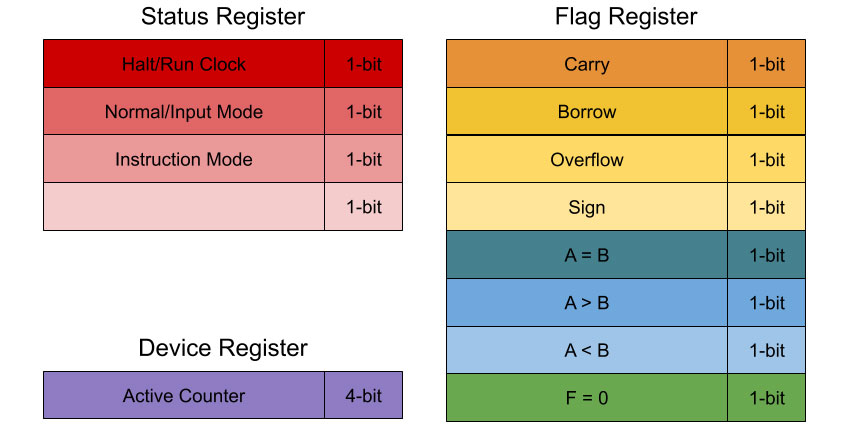
Halt / Run
This flag is used to determine in the clock run or not. When the clock is not running, the user can single-step through a program manually. Useful at the end of a program to preserve output, or during execution for breakpoints. Can be set by the user, by an instruction, or perhaps by an error (hopefully),
Normal / Input
In normal mode, the PC increments via the clock (or the single step button, if the clock is halted). When in input mode, the user is able to program the computer via front-panel controls.
Instruction Mode
This mode determines how an instruction is processed by the control logic. If the first digit of an instruction in RAM is a zero, the instruction is decoded from the instruction register. If the first digit of an instruction in RAM is a one, the remaining 15-bits are treated as an address, loaded into the firmware counter, and this flag is set. This flag will keep the firmware counter in control until a return instruction causes the PC to become active and continue executing instructions in RAM.
Active Counter
This 4-bit register indicates which counter is in charge of the address bus (effectively, which counter is the current program counter).
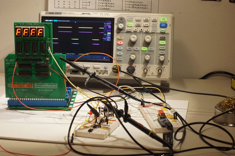
Successful Register Test
Bad breadboards have been the bane of this project, even when the circuits I am testing are on PCB. The last few register transfer tests failed because the data would corrupt or not actually save, and a few times the stored data in a register would change. I added 1k pull-downs to the data bus today, and it seemed to help, but constant glitches continued.
With the help of a new breadboard, I was able to successfully load values into Register-1, copy those values to Register-2, load a different value into Register-1 (clearing it, basically), then copy the value from Register-2 back to Register-1. I tested with the oscilloscope, and used the 16-bit display boards to see the values being moved around.
The next step is to build additional registers, then design the counters that will be used for memory addressing. Once we are at that stage, looping tests (driven by an arduino or raspberry pi) will be useful again.
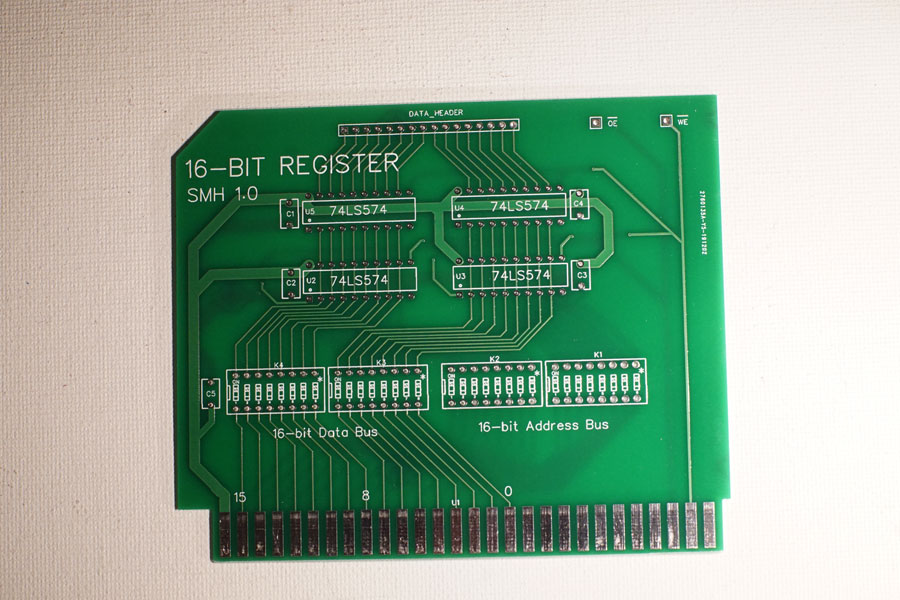
16-bit Register Board
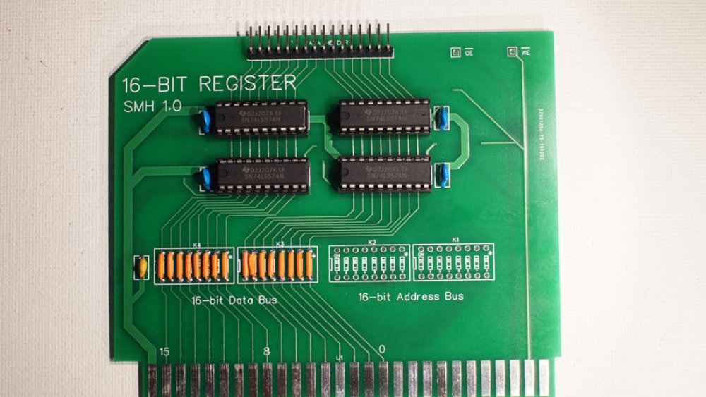
I had a lot of different plans for the 16-bit register, but all of them had two basic requirements:
- The PCB needs to work for both data-bus and address-bus registers.
- The PCB needs to have an "always on" header (for the front-panel or ALU)
I would prefer to design registers for specific uses, but when having PCBs manufactured it was more economical to try to combine designs as much as possible. Because of that, the PCB links the data and address-buses to the 74LS574 ICs, with breaks that I could jumper when populating the boards. To accomplish 3-state bus access but have the register value always available to a 16-pin header, I went with a second set of 74LS574s that store with the register ICs, but always outputs to the header. This adds about $2 to the cost of populating a register board, so in instances where the header might never be used, those extra ICs can be left out.
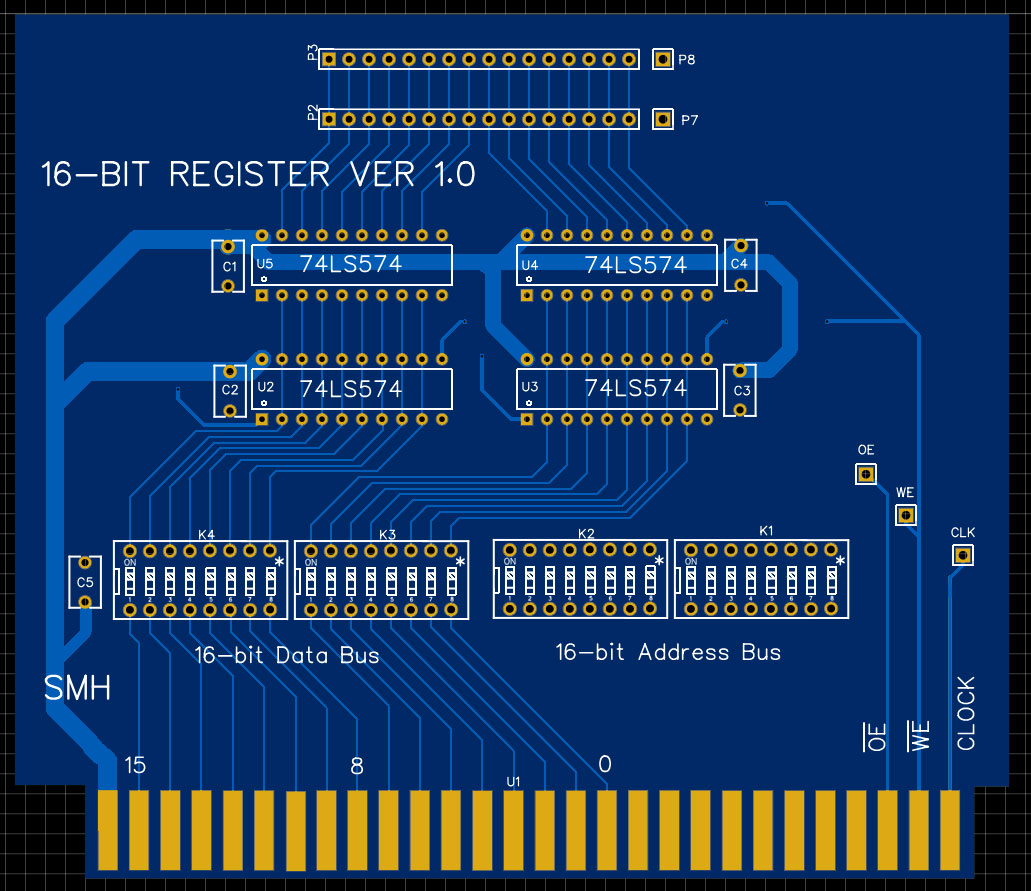
This design was created by hand as a PCB, without a schematic. I explain my reasoning in the Hex Display post, but basically I design PCBs the same way that I lay out breadboards... I grab the datasheets and start connecting pins. This is inefficient, and requires multiple iterations before I am happy with a design, but it feels better to me. In this case, this was not the final design but it makes an interesting contrast to what was produced. If you compare them, the main difference is how the signal test pins are located. The "clock" was dropped from this board, as the actual clock signal will be gated to this card and transmitted on the write enable line.
I also dropped the second 16-pin header on the top, as the display board was updated to act as a pass-through when necessary.
Fully populated, the register board was tested with my first display board. The oscilloscope probes are connected to the output of the 555 timer (on the foreground breadboard) and the clock test pin on the display board... I wanted to see how if the clock waveform deforms or picks up any noise. Unfortunately, when I took this photo I had the oscilloscope in "roll mode" so the waveform looks a bit dirty.
I have enough PCBs to build ten register boards, but I will start with three... A-Register and B-Register for the ALU, and one general purpose register. I might also populate an address register or two once I start programming branching and jumps.