16-bit Counter PCB Design

I have been struggling with planning the control logic of the computer, and a big part of that was handling the two buses. Some ICs, for example, the 74LS574 I use for registers, are 3-state. With a 3-state IC, the output can be disabled, and thus the inputs and outputs can be tied directly to a bus. In the case of the 74LS574 based registers, I want them to always output to a separate header, so I use transceivers to control access to the bus. With ICs that are not 3-state, we have no choice but to use transceivers, or they would always be outputting to the bus...even when we did not want them to. A second issue is that we need to separate the input from the output, otherwise these ICs output would interfere with the input values we want to store. Because of this, we need transceivers on both the input and output of our "card" to ensure that the card does not cause problems for other devices in the computer.
With a 16-bit data bus and a 16-bit address bus, I need four 74LS245 transceivers for 3-state devices, and six for the others. The cost of the extra transceiver ICs is not an issue (I have nearly sixty of them lol), but the PCB traces quickly get out of hand and the control logic to enable, disable, and set direction for all of them is complex.
The address bus has always been problematic in my design. I want to have multiple counters that can be enabled and disabled (for jumps, returns, etc), and I have multiple blocks of RAM and ROM that I want to be able to access. To that end, I have made the difficult decision to dispense with the address bus. This means that counter cards will need output headers (similar to the register cards), and new RAM or ROM cards will need to accept addressing from a similar header.

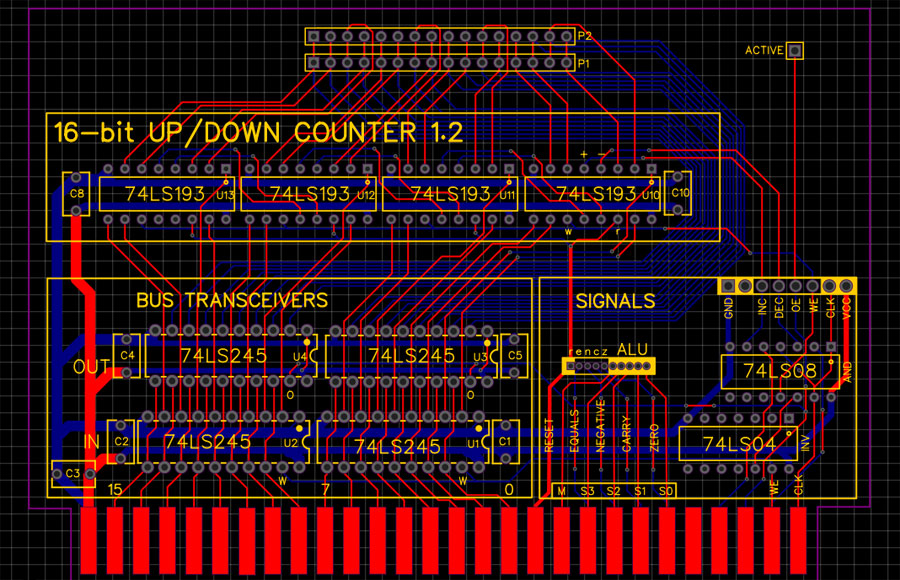
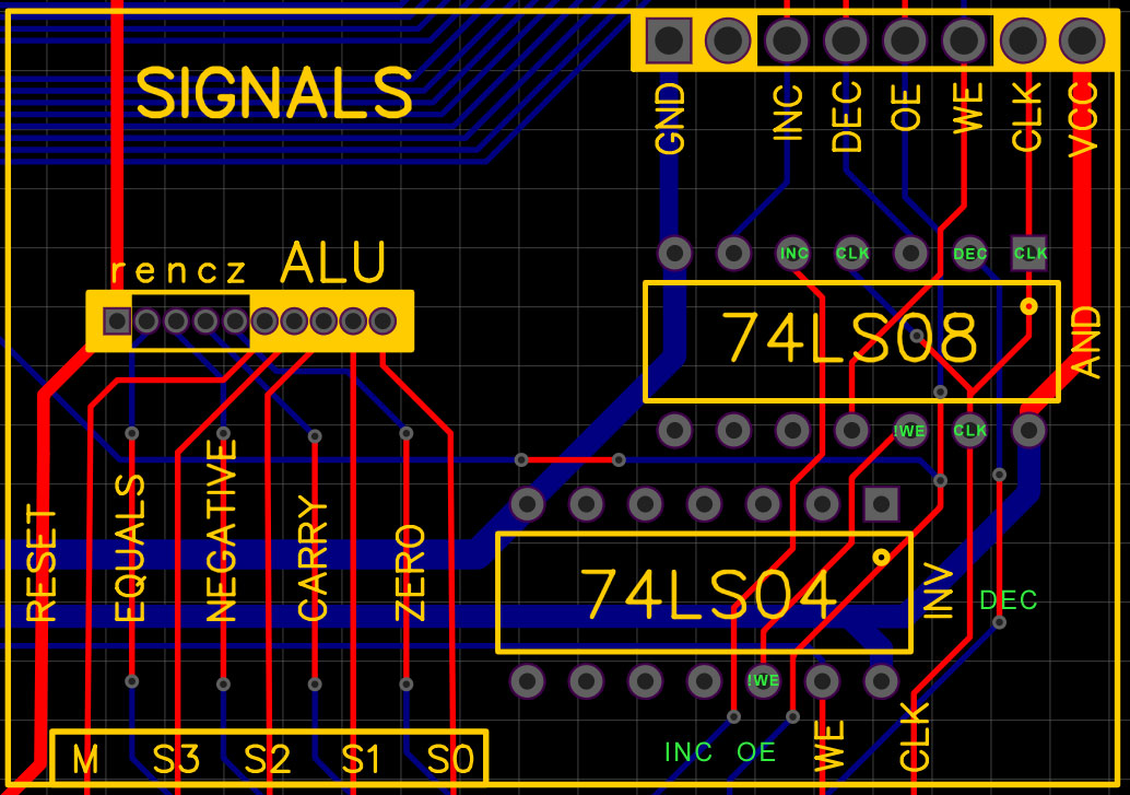
Without an address bus to worry about, we only need four transceivers, and because of that, we can stack them above the data bus and run all of the controls without any difficulty. The 74LS08 (quad AND gates) is used to gate the clock signals. If the WE signal is set, the CLK and !CLK signals are allowed through, otherwise no clock signals are available to the card. This has several benefits, including reducing the "fan out load" on the clock. All of the other signals and controls are passed through without buffering. The left controls (Flags and ALU lines) are only used on some cards, so buffering will only be added on appropriate cards. The right controls are not bused, so they do not need buffering. To keep things consistent, the "Write Enable" signal is active low (same as the Output Enable", but we need to invert it if we want to AND it with the clock. If the AND gate received a low "WE" signal, it would not pass the clock through, and thus no write would occur. We also need to and the Increment and Decrement signals with the clock, but those are already active high so we can bypass the hex inverter (74LS04). I have added some additional labels in green to make it easier to follow in the closeup shot.
