Bus Architecture - February 2020 Design
As I work through plans for the control logic and instructions, I realize that I need to simplify and streamline things. This does not mean lots of registers or segmented memory, or dropping a stack, but it does mean I am looking closely at how those things will work.
Six months ago, I was considering a two data bus, single address bus system with registers, pointers, memory, and even the ALU accessing at least two of the three buses. I like this because I could have an "A" and a "B" data bus that work as the inputs to the ALU. This simplified some things, and seemed like an elegant solution to the problems of moving data. Unfortunately, a three-bus system requires more control logic and a lot of transceivers, not to mention all of those extra traces that had to fit into two layers (I am not planning on moving to four-layer PCBs, lol).
Three months ago, I settled on a two bus system with address and data buses on the backplane. On paper this seemed the perfect solution, and seemed to be a common one in TTL based computers of the 70s and 80s. Again, there were difficulties with the two buses super-imposed on the backplane... complicated traces, extra transceivers, etc.
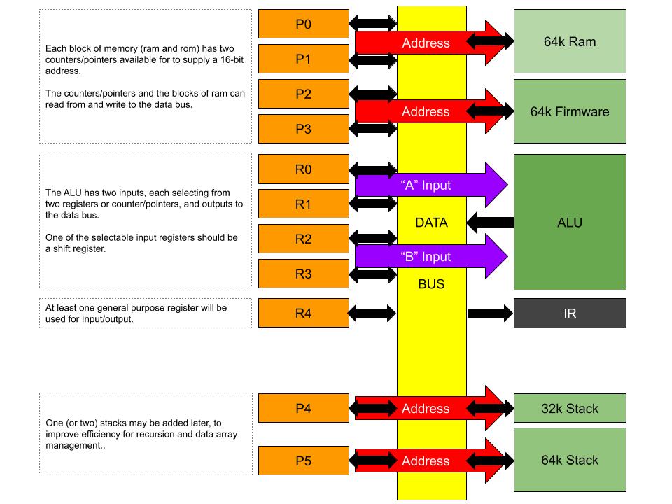
A more pressing concern with a common address bus is bus contention. I plan on having a bank of RAM, a bank of ROM, and later one of two Stacks. Each of these will need their own addressing, and if I want to be able to push a value onto a stack from RAM, it would be nice to have separate addressing so we can perform a single clock-cycle transfer (similar to copying values between registers).

With the exceptions of the Instruction Register and Arithmetic Logic Unit, every device can read from and write to the data bus. With separate addressing for the memory based devices, we can copy values from any device (again, except the IR and ALU) in a single step. RAM to Register, Register to Pointer, Pointer to Stack, Stack to RAM, etc. The control logic is pretty simple, with each device having a write and load signal to control access to the data bus. In the case of RAM and ROM, I plan to have two pointers that can be selected from. Until a Stack is added, this will be the only efficient method to store a "return address" when performing a jump. Even after a Stack has been added, this will be more efficient when recursion is not evident.
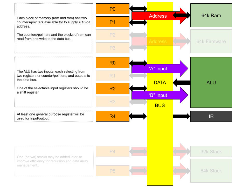
The ALU has two inputs, labeled "A" and "B". In this design, these will have a choice of one of two inputs, much like the address lines for the memory cards. Multiple possible inputs mean we can save juggling data between registers, and if one of those registers is an address pointer, it means the ALU can calculate jumps and write them back to the address pointer very efficiently.

To start, we will only need one bank of memory with the pointers, the ALU with two input registers, one general purpose register (for output), and the Instruction Register. This will be enough to get started with.
