ALU Instructions
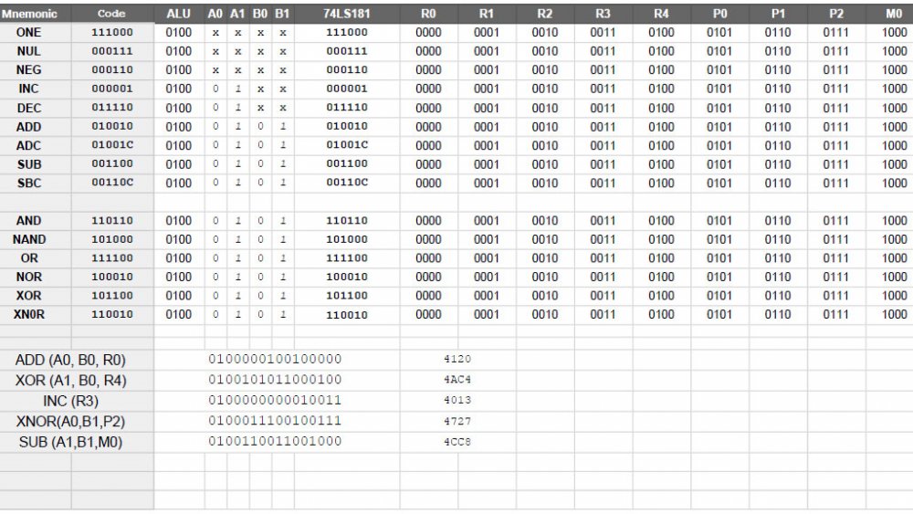
The 74LS181 is an interesting IC, but one of the benefits of it is the host of functionality it provides access to. This IC takes a mode signal to switch between logical and arithmetic functions, four signals to indicate the function, and a carry that changes what arithmetic functions are able to do. For example subtraction is either A - B or A - B - 1, depending on the carry flag.
In this computer, with 16-bit instructions, ALU operations are indicated by 0100, and perhaps 0101 (but I will speak about that in a future post, after some testing). These four digits lead the instruction, so (from a hexadecimal view), all ALU functions will start with a hex 4. The next two digits indicate source for the "A" register and "B" register inputs. When combined, this means the ALU function and source inputs take up 8-bits, and give us two hex digits in the middle. This is followed by the actual ALU instruction, which is six digits in total. Finally, a four digit target is included, making the target a human readable "0 - F".
Examples:
#4xx3 - ALU function xx, store the result in device 3
#4xxF - ALU function xx, store the result in device 15
#4xxA - ALU function xx, store the result in device 10.
The two hex digits for the function are more complicated, but should be human readable with a simple lookup table.
Non-ALU Plans
Each operation starts with a 4-bit system identifier, followed by a 4-bit function, and one or two 4-bit identifiers. This means other instructions should be human readable in hex format. Where a "system" needs more than sixteen possible functions, we can allocate additional "system" codes, or break the instructions up... conditional operations (like branching) might be organized into a separate block from unconditional operations (like jumps), and two-part operations (memory related) into their own as well.
Example:
#1xE7 - A "system 1" function, using device 14 as the source and device 7 as the target.
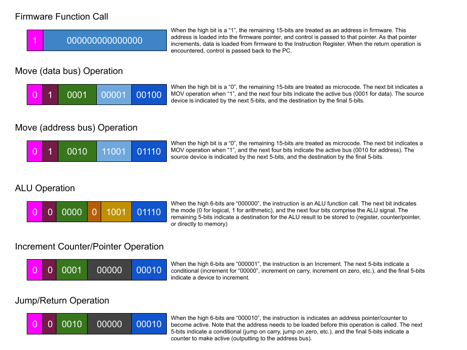
Instruction Design, 4-bit Device Identification
I want 5-bit identifiers so that I can have more than ample devices on the backplane, but the reality is coding will be much simpler with 4-bit chunks... each part of an instruction can be indicated with a single hexadecimal character.
.png)
The first digit of any actual instruction will be zero and can be ignored. The next 6-bits are the actual "instruction" in most cases, and is blocked in purple. The orange bit indicates a mode or status, and is not always required. The light blue block indicates a source device and the darker blue a destination or target device. A red block indicates the 4-bit ALU signal. The 4-bit black block indicates the source for conditionals... 0000 meaning the instruction is not conditional, 0001 meaning the instruction occurs when the carry flag is set, etc.
Instruction Parts Plan
I believe it will be easier to design and prototype the Instruction Register and control logic if I know what the instruction values will be, so I am prototyping the format of microcode. This image is subject to change, but really helps me to visualize microcode instructions.
MOV Instruction - 4-bit Device IDs
I will start with the plan for 4-bit device identification. This allows a source and destination to each be a single hex digit, making it much more human readable. Peripherals can be identified by their own 4-bit identifiers, with the leading instruction providing content. This means more leading instructions, but I believe it will be worth it... and sixteen devices will be sufficient to start anyway.
Device Binary Hex
0 0000 0
1 0001 1
2 0010 2
3 0011 3
4 0100 4
5 0101 5
6 0110 6
7 0111 7
8 1000 8
9 1001 9
10 1010 A
11 1011 B
12 1100 C
13 1101 D
14 1110 E
15 1111 F
I have three completed registers now, so it is possible to start prototyping the Instruction Register and the control logic for a MOV instruction to copy values from one register to the next. In the prototype, the IR can actually be 16-lane dip switches. To that end, I need to actually pick a code for the MOV instruction.
If the highest order bit is the instruction mode (1 for firmware address, 0 for microcode), that means that the first hex digit must be a 7 or less. Any value of 8 or higher will indicate that the remaining 15-bits are an address in the EEPROM bank.
OP Code Example Instruction Description
0A{sd} 0A1F MOV S, D Move a value from source to destination.
The control logic needs to decode this in parts. For now, I will assume the decoding is in 4-bit chunks.
0000 - Ignore
1010 - MOV
0001 - Source Device
1111 - Destination Device
MOV Instruction - 5-bit Device IDs
While 4-bit identifiers are straight forward to use, 5-bit identifiers greatly expand the potential of the computer. Using 10-bits to identify source and destination only leaves us with 6-bits for the rest of the instruction, 5-bits when we take the instruction mode bit into consideration. With three 5-bit pieces, we do not have a stable opcode for the "MOV" portion of the instruction... each hex character is made up of 4-bits.
Device Binary Hex
0 00000 0
1 00001 1
2 00010 2
3 00011 3
4 00100 4
5 00101 5
6 00110 6
7 00111 7
8 01000 8
9 01001 9
10 01010 A
11 01011 B
12 01100 C
13 01101 D
. . .
30 11110 FE
31 11111 FF
If the highest order bit is the instruction mode (1 for firmware address, 0 for microcode), that means that the first hex digit must be a 7 or less. Any value of 8 or higher will indicate that the remaining 15-bits are an address in the EEPROM bank.
The control logic needs to decode this in parts, and in this case it would be in unwieldy 5-bit chunks.
010000 - MOV
00001 - Source Device
01111 - Destination Device
An alternative to this would be to combine the source with the MOV instruction and make the destination 8-bits (padded with zeros from 5-bits)
M04, 1E - Move the value from device #4 into device #1E.
MFF, 09 - Move the value from device #FF into device #9
I do not like this, it is not an elegant solution, it wastes instruction bits, and it means numerous duplicate instructions. I think I need to stick to 4-bit identifiers. Fifteen devices (plus the zero register) will limit the number of devices I can use effectively with the MOV instruction, but other instructions may be more flexible..
Instruction Length and Components
For register to register type instructions, I wanted to go with 5-bit identifiers. This leaves 6-bits for the command, and allows for thirty-two connected devices. This may be overkill, as 4-bit identifiers still gives us sixteen devices (0-15), and each device is identified by a single hex value.
The best way to see why this might matter is to compare three MOV instructions, copying values between two registers. With 4-bit identifiers (the left hex instruction) the first two characters indicate the command and the next two a source and destination device. When we use 5-bit identifiers (the right hex instructions), only the first character will be unchanged, the next three will vary depending on the actual device IDs.
4-Bit 5-bit
MOV R01, R10 AA1A vs A82A
MOV R13, R11 AADB vs A9AB
MOV R00, R15 AA0F vs AA0F
It probably does not matter in the long run, I may be using an assembler, but the left examples are clearer and easier to understand than the right.
I will have to give this some thought, as I am not sure 16 devices (15, really) will be enough. Hypothetically speaking, I will need the following:
Planned Device List
0 - Zero/Null Register
1 - Program Counter
2 - Return Register
3 - Firmware Pointer
4 - Firmware Return Register
5 - Variable Pointer
6 - Loop Counter
7 - "A" Register, for ALU
8 - "B" Register, for ALU
9 - General Purpose Register
A - 64K of user programming memory
B - 64k of variable storage memory
C - 64k of firmware
A possibility would be to combine device B and C into one, with 32k of eeprom and 32k of sram. This would be a compromise, but would free a device number.
This is pretty tight, considering it does not include I/O of any kind, any front-panel registers, sound or video systems... but those may work okay as dedicated instructions. This is how the ALU will work.. it does not have a Device ID per say, instead an ALU instruction includes 5-bits for the mode and signals, and 4-bits for a destination device on the data bus. Sound systems, video, LCD output, etc. will probably interface via special registers, but they may not need device numbers the way memory banks or normal registers do. If I go with 5-bit identifiers, we would have twice as many device numbers available and could easily include a dozen different addressable registers.
Microcode - Machine Language - Higher Level Language Example
It is too early to do this justice, but I wanted an example of how the different levels of code might compare. This example is very simple, as each version stores a decimal value of 4096 to a variable (assuming the variable is already setup so that it is usable). Variables are abstracted, but should work like registers, with the ability to read and write to them, perform math functions on them, etc.
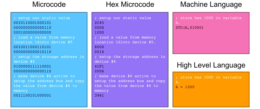
At a high level, we want to be able to say "put 1000 into variable A", but at lower levels we are forced to work with actual memory addresses, physical registers, etc. The difference in complexity is obvious, but to get to a high level language we need to write language functions (like variable read and write) in lower level code and then call them by their starting address in the firmware. Where higher level functions require passing values, we need to setup stacks or registers with the appropriate values so that the function will have what it needs. Functions will often need to update registers or locations in memory, so standards need to be developed and adhered to.
I will go into firmware memory segmentation in the next post, as it is an important concept to get across clearly.
Memory Segmentation and Firmware Plans
When I switched to a 16-bit data word, I had to rethink how instructions would work. Not at the lowest level, I still need to have ways to identify two registers and move data between them... but at a higher level. Can a branch be a single microcode instruction?
As a programmer, I like to think in terms of instructions, and some of the first programming I ever did was in 6502 machine language. Not assembly, I hand coded machine language by poking hex numbers into memory. To make my computer "usable", I need a way to get to a machine language level, so I can have a single instruction that can read or change a value in memory, or multiply two numbers, or compare the values of variables (instead of registers). Basically, I need a programming language. I also need a rudimentary operating system, to provide a bit of a framework for reading input, loading and saving programs, etc. To accomplish this, I am planning on segmented and overlapping memory, where 64K of SRAM and 64K of EEPROM occupies the same address space.
The user code space, in 64k of RAM, will be looked at in more detail at a later time, but it will probably contain some reserved blocks as well. The firmware side is the main subject of this post, so we will concentrate on that.
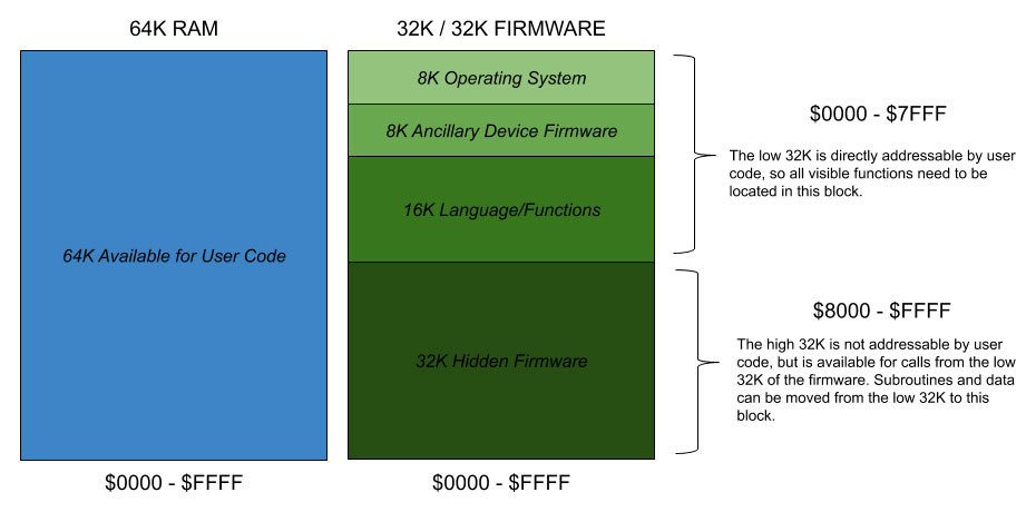
Instructions, in RAM, will include a 1-bit mode flag that will indicate whether it is a microcode instruction (see the "Parts of an Instruction" post for examples) or a language instruction call (basically, the starting address of a block of code in firmware). With 16-bit words, and a 1-bit mode flag, we have 15-bits remaining as a firmware address. This allows user available instructions to start in the low 32K of firmware. And additional 32K of "hidden" firmware is available for storing subroutines, code modules, and data required by instructions located in the user addressable space.
When a user program makes a call to a "language instruction" in firmware, the address is loaded into a separate firmware address pointer, leaving the PC pointing to the next instruction. The firmware address pointer will take over control of the computer, and will increment as microcode is loaded into the Instruction Register and executed. When a "return" is hit, the PC is activated again and the user program continues on. This basically allows users to mix microcode and higher level instructions at will. A future version may drop microcode support, at which time the entire 64K (or an additional bank, for 128K of Firmware) would be user addressable.
I considered having all user available instructions simply be addresses to the firmware, but 32k addressable seems like enough and I plan to build the language one instruction at a time in ram and move them to the firmware as they are perfected. That said, the goal is to have a simple high-level language based on basic, python, or c for users, with machine language mainly used to create new language instructions. Microcode probably will not be used in user programs once easier-to-use options are available.
I will give a theoretical example in the next post that will show how the same functionality could be implemented in the three levels of code. In a subsequent post, I will into more detail regarding the planned segmentation of the firmware into OS, reserved for peripherals, and language blocks. Planning ahead of time will make things much easier to work with later.
Parts of an instruction
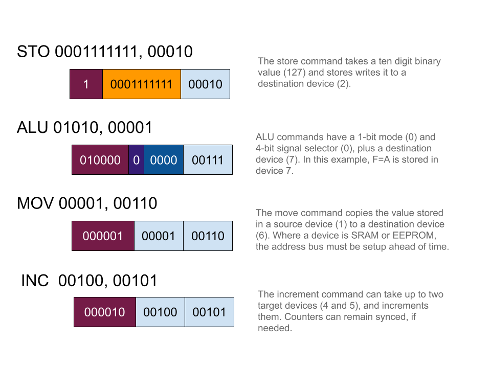
I am still trying to figure out the best format for instructions, and it looks like they will have variable length verbs. For a store command, I think one flag digit and five destination digits are sufficient, and allow for a ten digit binary value. When we are copying values between devices, a total of ten digits are required to identify the two devices. For something like an increment command, we only need five digits for the target... but we have room for two, and it might be useful for syncing counters (coping a range of values from EEPROM to SRAM, for example) so why not allow up to two counters to increment at a time?
This is all subject to change, but working through possible instruction structures is definitely useful.
Device ID Codes
The actual identifications will be assigned later, when the hardware is assembled most likely, but this will be a helpful guide as I work out the backplane (currently considering three options between 56 and 80 lanes).
| Device ID | Signals/Commands | Description and Notes |
| 00000 | we,oe | Zero/Null Register |
| 00001 | we,oe | A-Register, half of the ALU input |
| 00010 | we,oe | B-Register, half of the ALU input |
| 00011 | we,oe, inc | Program Counter |
| 00100 | we,oe | SRAM, 64k bank 1 |
| 00101 | we, oe | General purpose data register (temporary value storage?) |
| 00110 | we, oe | General purpose data register (output register?) |
| 00111 | we, oe | General purpose address register (branch address?) |
The idea is we can identify most devices using a 5-digit code. If we start with nine devices, we will have an ALU, 64k of memory, and four general purpose registers to work with.
The Instruction Register is not listed above as there will be no instructions that affect it directly. The ALU does not need an identifier, either. We can use the 5-digits of the "source" to pass the ALU a mode (1-bit flag to switch between logical and mathematical functions) and command (4-bit signal to indicate which of sixteen functions to execute).
To start, a minimal setup would need the following five addressable devices, plus the Instruction Register and ALU.
| Device ID | Signals/Commands | Description and Notes |
| 00000 | we,oe | Zero/Null Register |
| 00001 | we,oe | A-Register, half of the ALU input |
| 00010 | we,oe | B-Register, half of the ALU input |
| 00011 | we,oe, inc | Program Counter |
| 00100 | we,oe | SRAM, 64k bank 1 |
Note that the "Zero Register" might not actually be a card, it could be pull down resistors directly soldered to the backplane, as long as no actual device is assigned the 00000 identifier. The Instruction Register will need to reside on the data bus as well, but is not included in the above as it is not accessible to instructions (i.e. there are no software instructions to manipulate the IR). The ALU is not addressed by a device number, but will still need to take up a slot on the backplane to output results.
16-bit Instruction Plans... Rough Draft?
I finally decided to go with a full 16-bit computer, after four years of prototyping an 8-bit system. Why? Well, 16-bit instructions give us a lot of "resources" to work with, without having to split instructions across multiple words. 16-bit registers and ALU simplify a lot of maths, and make it trivial to manipulate addresses. 16-bit instructions also simplify a lot of hardware concerns, including breaking instructions up over several IR fetches and very limited identifiers for devices (registers, SRAM, etc.)
With 16-bits to work with, we are able to dedicate 5-bits to identification giving us a maximum of thirty-two devices. For example, the "A-Register" may be device 00001, while an SRAM bank may be device 00110. Device 00000 will be the "Zero-Register, effectively identifying no device and allowing the pull down resistors to control the bus.
Examples
With 5-bit identification, the first instruction to consider is a MOV, or copy instruction between two devices.
MOV 00001 00010 - Output Enable for device 1, and Write Enable for device 2
Source and destination identifiers take up ten binary digits, leaving six more, so these six will be available for all move/copy instructions. Where a source and destination are not required... an increment instruction, for example... more digits are obviously available. So, knowing this, how do we decide how an instruction is laid out?
MOV Instruction
We need five digits for the source and five digits for the destination when moving or copying values between devices. This can be as simple as copying values between two registers. Note that this also works for SRAM, EEPROMs, etc, except that in those cases the addressing needs to be setup ahead of time.
   Source  Destination

   00001    01110
STO Instruction
A store instruction immediately stores a value, encoded as part of the instruction, to the destination device. The first bit of an instruction can be used to determine when an immediate store is called, the next ten digits (numbers up to 1023) are the value, and the final five digits are the destination device.
   Value      Destination

   0000000010 11001
ALU Instruction
Assuming the ALU is always connected to the A-Register and B-Register as inputs, we can assign 5-digits to the mode and signals, with the other 5-digits indicating a destination to store the result.
   Mode  Signal  Destination

   0     0001    01110
Because instructions can be variable... we do not always have a "source" device, for example... it is important to create a sensible guide.
1vvvvvvvvvvyyyyy - Store the 10-bit value "vvvvvvvvvv" into the "yyyyy" device. This may often be an 8-bit number, but 10-bits can be available in this instruction and those extra bits are the difference between a maximum of 255 and 1023.
010000xxxxxyyyyy - Write the 16-bit value stored in the "xxxxx" device to the bus, and write that value to "yyyyy".
001000mssssyyyyy - Execute the ALU function indicated by mode "m" and signal "ssss". and write the 16-bit result to the "yyyyy" device.
This is just a start, but I do like 5-digit identifiers as that means we can have 32 devices... way more than needed. The original 8-bit design was going to have 3-digit identifiers, limiting us to nine separate devices. That can work, but is limiting and would greatly impact the difficulty of hand-coding useful software. With thirty-two devices, we can have the ALU, A-Register, B-Register, several general purpose data and address registers, several address pointers (including the Program Counter), multiple banks of SRAM and EEPROMs... even things like sound and video cards, or input devices.
I need to give some thought to conditionals... branches, jumps, whatever we want to call them. These commands will follow a similar design as above, but will be conditional based on a flag (carry, negative, zero, etc). The remainder of the instruction can be an offset (requiring the ALU to calculate a destination address by adding or subtracting that offset from the PC), or perhaps a device containing that address (a Jump Register is loaded with an address, then that address is put onto the address bus *if* the condition is met.