Connection/Development Board
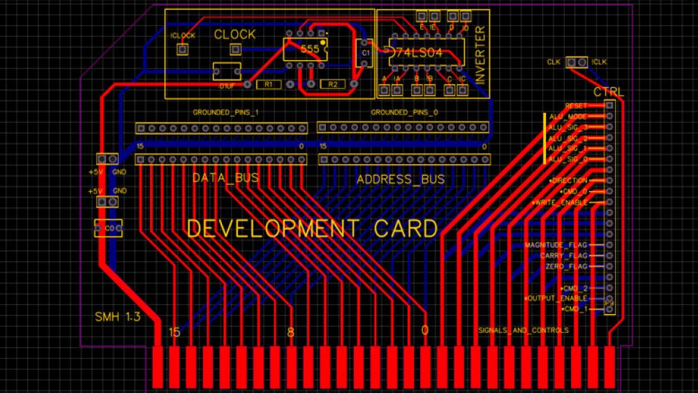
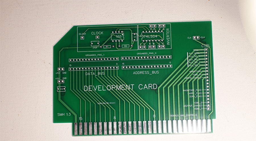
One of the issues when moving from breadboard to PCB is coming up with an interface between the two. To that end, I came up with a simple connection/development board that breaks all of the backplane lanes out to headers. To make development and testing easier, I added a 555 circuit, a hex inverter, and an extra set of grounded headers. The purpose of the grounded headers is to allow one of these boards to act as terminating resistors, pulling the buses low as a default. The 555 timer circuit allows us to have development clocks that can optionally be tied to the clock lanes of the backplane (again, via pin headers).
The main purpose of the connector board is to make it easy to connect to breadboards, so all of the headers are clearly labeled. Where labels are missing, the lane has not yet been assigned.
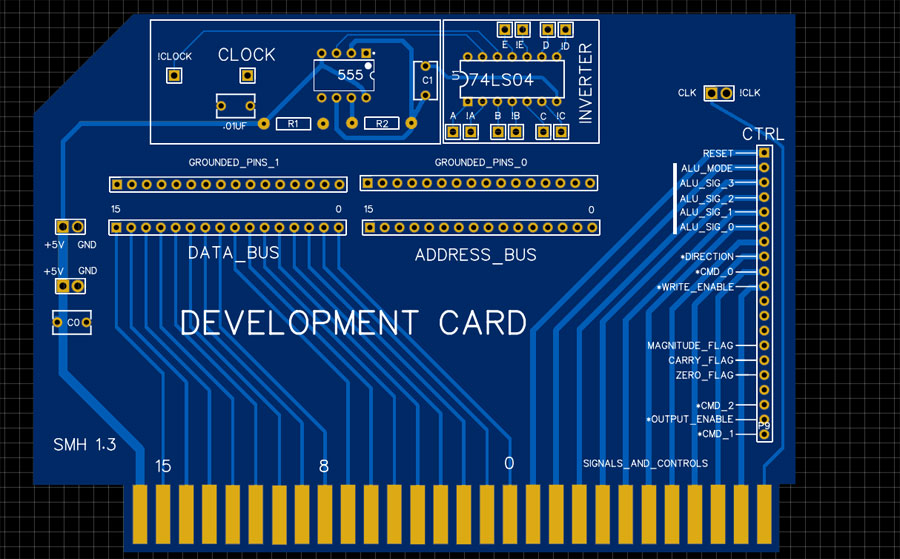
The most interesting part of this card is the labeled control header, as it sets a lot of things in stone. The rightmost connector lane is a common clock signal (on both sides of the card), but the next pads are not shared lanes, they are linked to the selector headers on the backplane. The rest of the signals and controls are lanes, including the ALU signals and the various flags. When I designed the board I was planning a minimum of three flags and was not sure what the third was going to be (A = B, A > B, A < B, Negative, etc), so I labeled it as the "Magnitude Flag", but it turns out that combining it with the carry flag can give us all three. There is room for more shared flags and controls.
Downloads
Connection Card 1.2 Gerber File