Backplane Connector Pinout (Schematic)
One of the nice things about designing PCBs to replace breadboards is we are forced to make decisions. Once a PCB is manufactured, it is not easy to make changes, where a breadboard is almost by definition always changing. This means that I am forced to finalize designs, so that all of the PCBs will work correctly.
In the case of the backplane, and the modified JAMMA connectors, there is some flexibility. I do not need to assign a purpose to every lane, but the shared lanes that are assigned must be respected by every card or device attached to the backplane. This has resulted in a series of pinout schematics, with the most recent displayed below.
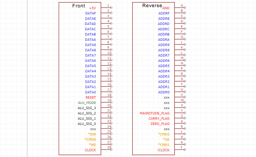
The front of the connector, and any PCBs inserted into the connector, is dominated by +5V, the 16-bit data bus, and the ALU signal lanes. The reverse is side has Ground, the 16-but address bus, and the flags. Each side also has three isolated breakout pins that are not shared between connectors. Note that the OE and WE pins are on opposite sites... this was caused by a layout error on the register card that was most easily fixed by reassigning the location of OE... even if it seems a little random when viewing the pinout. Whoops.
The "Reset" line is planned to be both user triggered (when the computer is turned on, or when a reset button is pressed) as well as software triggered. The purpose of reset would be to clear registers and set counters back to zero, so that a program can start "fresh". The software triggered reset is planned for future use... perhaps after a program is transferred from storage to ram, we clear the registers and start the program counter at the start of the program. In the case of "Reset", I plan to have a special purpose register that is not cleared... so that a program can react differently based on the contents of that register.
The ALU signals will be discussed at length elsewhere, but basically we have a mode flag that switches the 74LS181 ALU ICs between logical and mathematical functions, plus four command signals that select one of sixteen functions.
The six breakout pins, in orange, are unique to each card and can be assigned to anything, but the Write Enable and Output Enable are common for most devices so those are labelled. The DIR pin, and the three CMD pins are effectively unassigned at this time.