06 - Other Hardware
Front Panel Instruction Indicators - Cardboard Prototype
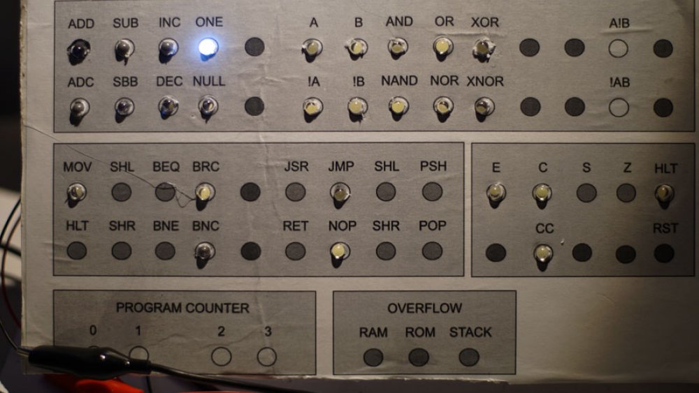
It is pretty rough, but this cardboard prototype of the "Instruction Indicators" panel will be pretty useful when I am working on control logic. I am working on the computer instructions / operations, and this will greatly speed development and allow easy confirmation that the control signals are correct.
Making a prototype was also helpful to identify some issues with the current design, including how impossibly bright the LEDs are. The illuminated LED in the above photo has two layers of opaque plastic covering it. I will be experimenting with dips and coating in the coming weeks, but the best option may be to power the LEDS from a separate 3-volt system to improve the lifespan of the LEDs.
Status and Control Register
There are various flags that need to be set for the computer to work correctly, such as a carry flag when an arithmetic operation results in a value larger than 16-bits.
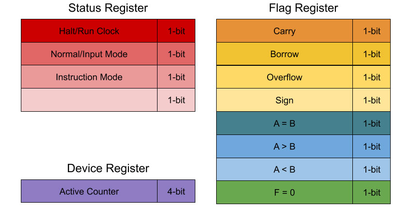
Halt / Run
This flag is used to determine in the clock run or not. When the clock is not running, the user can single-step through a program manually. Useful at the end of a program to preserve output, or during execution for breakpoints. Can be set by the user, by an instruction, or perhaps by an error (hopefully),
Normal / Input
In normal mode, the PC increments via the clock (or the single step button, if the clock is halted). When in input mode, the user is able to program the computer via front-panel controls.
Instruction Mode
This mode determines how an instruction is processed by the control logic. If the first digit of an instruction in RAM is a zero, the instruction is decoded from the instruction register. If the first digit of an instruction in RAM is a one, the remaining 15-bits are treated as an address, loaded into the firmware counter, and this flag is set. This flag will keep the firmware counter in control until a return instruction causes the PC to become active and continue executing instructions in RAM.
Active Counter
This 4-bit register indicates which counter is in charge of the address bus (effectively, which counter is the current program counter).
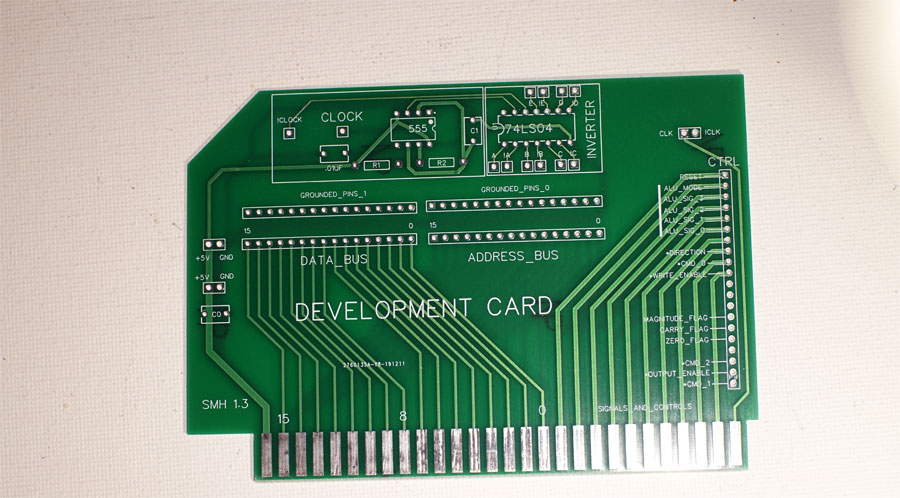
Connection/Development Board #1
The first connection board has been partially assembled and was ready for the first round of tests to make sure my timer circuit works. For this first board, I setup a 10Hz astable 555 timer, with the the output going to a test pin. The output also goes to a 74LS04 hex inverter to give me a second, inverted, clock signal.
I tested by hooking channel 1 (yellow trace) of the oscilloscope to the 555 output, and channel 2 (purple) to the inverted 555 output.
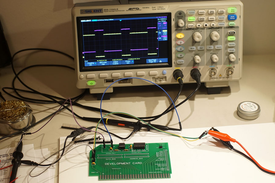
I adjusted the two channels to make it easy to see the two square waves, and it looks pretty good. The only possible concern is what appears to be a fair bit of noise when the signals are low. The long, unshielded test leads are probably responsible, but I plan on further testing.
All that remains is to solder on the 16-pin headers and this first connection/development board will be complete.
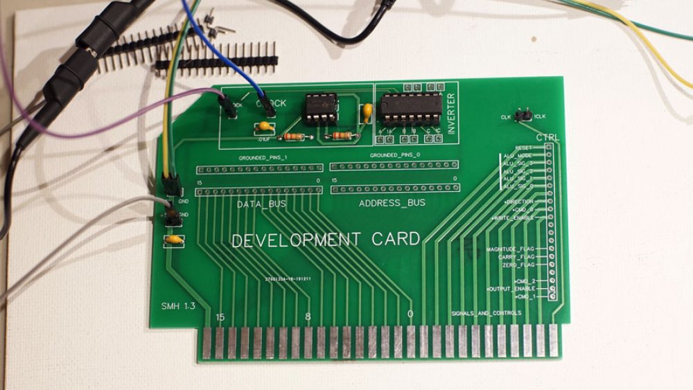
Connection/Development Board
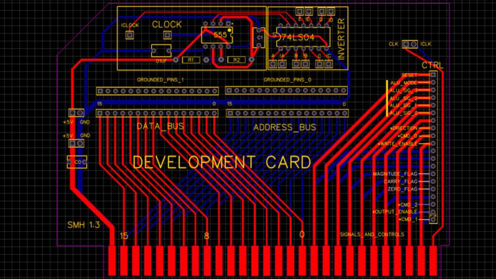
One of the issues when moving from breadboard to PCB is coming up with an interface between the two. To that end, I came up with a simple connection/development board that breaks all of the backplane lanes out to headers. To make development and testing easier, I added a 555 circuit, a hex inverter, and an extra set of grounded headers. The purpose of the grounded headers is to allow one of these boards to act as terminating resistors, pulling the buses low as a default. The 555 timer circuit allows us to have development clocks that can optionally be tied to the clock lanes of the backplane (again, via pin headers).
The main purpose of the connector board is to make it easy to connect to breadboards, so all of the headers are clearly labeled. Where labels are missing, the lane has not yet been assigned.
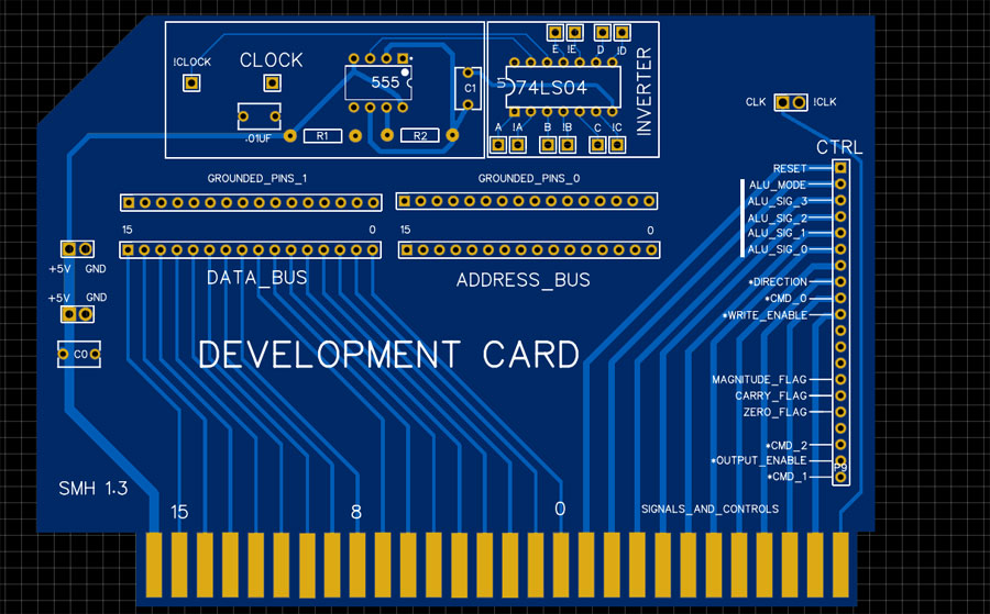
The most interesting part of this card is the labeled control header, as it sets a lot of things in stone. The rightmost connector lane is a common clock signal (on both sides of the card), but the next pads are not shared lanes, they are linked to the selector headers on the backplane. The rest of the signals and controls are lanes, including the ALU signals and the various flags. When I designed the board I was planning a minimum of three flags and was not sure what the third was going to be (A = B, A > B, A < B, Negative, etc), so I labeled it as the "Magnitude Flag", but it turns out that combining it with the carry flag can give us all three. There is room for more shared flags and controls.
Downloads
Connection Card 1.2 Gerber File